ADNK-5033-FS27 Avago Technologies US Inc., ADNK-5033-FS27 Datasheet - Page 2
ADNK-5033-FS27
Manufacturer Part Number
ADNK-5033-FS27
Description
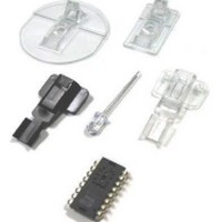
KIT REF DES OPT MOUSE ADNS-5030
Manufacturer
Avago Technologies US Inc.
Datasheets
1.ADNK-5033-FS27.pdf
(24 pages)
2.ADNK-5033-FS27.pdf
(6 pages)
3.ADNK-5033-FS27.pdf
(32 pages)
Specifications of ADNK-5033-FS27
Main Purpose
Reference Design, Optical Mouse
Utilized Ic / Part
ADNS-5030
Wireless Frequency
27 MHz
Interface Type
USB
Modulation
FSK
For Use With/related Products
MC68HC908QY4A, MC68HC908JB12
Lead Free Status / RoHS Status
Lead free / RoHS Compliant
Secondary Attributes
-
Embedded
-
Primary Attributes
-
Lead Free Status / Rohs Status
Lead free / RoHS Compliant


Mouse Buttons
Mouse buttons are connected as standard switches.
These switches are pulled up by the pull up resistors
inside the microcontroller. When the user presses a
button, the switch will be closed and the pin will be
pulled LOW to GND. A LOW state at the pin is
interpreted as the button being pressed. A HIGH state
is interpreted as the button has been released or the
button is not being pressed. Normally the switches are
debounced in firmware for 15-20ms. In this reference
design there are three switches: left, Z-wheel, and right.
Optical Navigation Sensor
Avago Technologies ADNS-5030 optical sensor is used
in this reference design as the primary navigation
engine. This Optical Navigation Technology contains
an Image Acquisition System, a Digital Signal Processor,
and a four-wire serial port. The MC68HC908QY4A USB
microcontroller periodically reads the ADNS-5030’s
Delta_X and Delta_Y registers to obtain any horizontal
and vertical motion information happening as a result
of the mouse being moved.
This motion information will be reported to the PC to
update the position of the cursor. The advantages of
using ADNS-5030 optical sensor are the efficient power
management, high tracking accuracy, and flexibility of
programming the optical sensor via the SPI port.
Features include:
• Precise optical navigation technology
• No mechanical moving parts
• Smooth surface navigation
• Auto frame speed
• Accurate motion up to 14ips
• 500/1000 cpi resolution selection
• High speed motion detector
• Single 3.3 volt power supply
• Power conversation mode during times of no
• On chip LED drive with regulated current
• On chip resonator
• Serial port registers
To learn more about sensor’s technical information,
please visit the Avago Technologies web site at:
http://www.avagotech.com.
2
movement
− Programming
− Data transfer
Freescale MC68HC908QY4A and MC68HC908JB12
The MC68HC908QY4A and MC68HC908JB12 are
members of the low-cost, high-performance M68HC08
Family of 8-bit microcontroller units (MCUs). The
M68HC08 Family is a Complex Instruction Set
Computer (CISC) with Von Neumann architecture. All
MCUs in the family use the enhanced M68HC08 central
processor unit (CPU08) and are available with a veriety
of modules, memory sizes and types.
HC08 Features include:
• High-performance M68HC08 CPU core
• Fully upward-compatible object code with
• In-circuit FLASH programming
• Low-voltage inhibit (LVI)
• Power-on reset
• Power saving stop and wait modes
Special Features for MC68HC908QY4A:
• 5-V and 3-V operating voltages (VDD)
• 8-MHz internal bus operation at 5 V, 4-MHz at 3V
• Trimmable internal oscillator
• Auto wakeup from STOP capability
• 4096 bytes of –on-chip Flash memory with security
• 128 bytes of on-chip random access memory (RAM)
Special Features for MC68HC908JB12:
• 5-V operating voltages (VDD)
• 6-MHz internal bus frequency
• 12288 bytes of on-chip Flash memory with Security
• 384 bytes of on-chip random access memory (RAM)
• Universal Serial Bus specification 2.0 low-speed
M68HC05 Family
− 3.2 MHz internal bus operation
− 8-bit trim capability allows 0.4% accuracy
− ± 25% untrimmed
feature
feature
functions
− 1.5Mbps data rate
− On-chip 3.3V regulator
− Endpoint 0 with 8-byte transmit buffer and
− Endpoint 1 with 8-byte transmit buffer
− Endpoint 2 with 8-byte transmit buffer and
8-byte receive buffer
8-byte receive buffer
Related parts for ADNK-5033-FS27
Image
Part Number
Description
Manufacturer
Datasheet
Request
R

Part Number:
Description:
KIT REFERENCE DESIGN ADNK-5030
Manufacturer:
Avago Technologies US Inc.
Datasheet:

Part Number:
Description:
A2700 Sample Kit
Manufacturer:
Avago Technologies US Inc.
Datasheet:

Part Number:
Description:
OPTOCOUPLER GATE DRV 2A 16-SOIC
Manufacturer:
Avago Technologies US Inc.
Datasheet:
Part Number:
Description:
OPTOCOUPLER 2CH 2.5A 16-SOIC
Manufacturer:
Avago Technologies US Inc.
Datasheet:

Part Number:
Description:
OPTOCOUPLER GATE DRV 0.4A 16SOIC
Manufacturer:
Avago Technologies US Inc.
Datasheet:

Part Number:
Description:
OPTOCOUPLER 2.0A 250KHZ 8-DIP
Manufacturer:
Avago Technologies US Inc.
Datasheet:

Part Number:
Description:
OPTOCOUPLER 2.0A 250KHZ GW 8-SMD
Manufacturer:
Avago Technologies US Inc.
Datasheet:

Part Number:
Description:
OPTOCOUPLER 2CH 15MBD 3.3V 8SOIC
Manufacturer:
Avago Technologies US Inc.
Datasheet:
Part Number:
Description:
OPTOCOUPLER DARL-OUT 8-DIP
Manufacturer:
Avago Technologies US Inc.
Datasheet:
Part Number:
Description:
OPTOCOUPLER IGBT DRIVE 0.4A 8DIP
Manufacturer:
Avago Technologies US Inc.
Datasheet:
Part Number:
Description:
OPTOCOUPLER DARL-OUT 8-DIP
Manufacturer:
Avago Technologies US Inc.
Datasheet:

Part Number:
Description:
OPTOCOUPLER 1CH 1MBS 8-SMD GW
Manufacturer:
Avago Technologies US Inc.
Datasheet:
Part Number:
Description:
OPTOCOUPLER GATE DRIVER 8-DIP
Manufacturer:
Avago Technologies US Inc.
Datasheet:

Part Number:
Description:
OPTOCOUPLER GATE DRIVER 8-SMD
Manufacturer:
Avago Technologies US Inc.
Datasheet:

Part Number:
Description:
OPTOCOUPLER PHOTOTRANS 4-SMD
Manufacturer:
Avago Technologies US Inc.
Datasheet: