CDB5376 Cirrus Logic Inc, CDB5376 Datasheet - Page 15
CDB5376
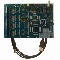
Manufacturer Part Number
CDB5376
Description
EVALUATION BOARD FOR CS5376
Manufacturer
Cirrus Logic Inc
Datasheets
1.CS5371A-ISZR.pdf
(32 pages)
2.CS4373A-ISZ.pdf
(34 pages)
3.CS5376A-IQZR.pdf
(106 pages)
4.CDB5378.pdf
(16 pages)
5.CDB5376.pdf
(80 pages)
6.CDB5376.pdf
(16 pages)
Specifications of CDB5376
Main Purpose
Seismic Evaluation System
Embedded
Yes, MCU, 8-Bit
Utilized Ic / Part
CS3301A, CS3302A, CS4373A, CS5372A, CS5376A
Primary Attributes
Quad Digital Filter
Secondary Attributes
Graphical User Interface, SPI™ & USB Interfaces
Processor To Be Evaluated
CS330x, CS4373A, CS537x
Interface Type
USB
Lead Free Status / RoHS Status
Contains lead / RoHS non-compliant
Lead Free Status / RoHS Status
Lead free / RoHS Compliant, Contains lead / RoHS non-compliant
Other names
598-1778


3.2 Decimated 24-bit Output
When the CS5371A and CS5372A modulator
operates with the CS5376A digital filter, the fi-
nal decimated, 24-bit, full-scale output code
range depends if digital offset correction is en-
abled. With digital offset correction enabled
within the digital filter, amplifier offset and the
modulator internal offset are removed from the
final conversion result.
3.3 Synchronization
The modulator is designed to operate synchro-
nously with other modulators in a distributed
measurement network, so a rising edge on the
MSYNC input resets the internal conversion
state machine to synchronize analog sample
timing. MSYNC is automatically generated by
the CS5376A digital filter after receiving a syn-
chronization signal from the external system,
and is chip-to-chip accurate within ± 1 MCLK
period.
DS748F3
> + (VREF+5%)
+ VREF
0 V
- VREF
> - (VREF+5%)
Analog Input
Table 1. 24-Bit Output Coding for the CS5371A
and CS5372A Modulator and CS5376A Digital
Differential
Modulator
Signal
Filter Combination
Corrected
A2EBE0
5D1420
000000
Offset
CS5376A Digital Filter
24-Bit Output Code
Error Flag Possible
Error Flag Possible
FDC420
5AD840
A527C0
-60 mV
Offset
5BC688
FEB268
A43978
-35 mV
Offset
3.4 Idle Tones
The CS5371A and CS5372A are delta-sigma-
type modulators and so can produce “idle
tones” in the measurement bandwidth when
the differential input signal is a steady-state
DC signal near mid-scale. Idle tones result
from low-frequency patterns in the output data
stream and appear in the measurement spec-
trum as small tones about -135 dB down from
full scale.
If the OFST pin is pulled high, idle tones are
eliminated within the modulator by adding
-60 mV (channel 1 of CS5371A and CS5372A)
or -35 mV (channel 2 of CS5372A) of internal
differential offset during conversion to push
idle tones out of the measurement bandwidth.
Care should be taken to ensure external offset
voltages do not negate the internally added
differential offset, or idle tones will re-appear.
3.5 Stability
The CS5371A and CS5372A ΔΣ modulators
have a fourth-order architecture which is con-
ditionally stable and may go into an oscillatory
condition if the analog inputs are over-ranged
more than 5% past either positive or negative
full scale.
If an unstable condition is detected, the modu-
lator collapses to a first-order system and tran-
sitions the MFLAG output low-to-high to signal
an error condition to the CS5376A digital filter.
The analog input signal must be reduced to
within the full-scale range for at least 32 MCLK
cycles for the modulator to recover from an os-
cillatory condition. If the analog input remains
over-ranged for an extended period, the mod-
ulator will cycle between fourth-order and first-
order operation and the MFLAG output will be
seen to pulse.
CS5371A CS5372A
15
Related parts for CDB5376
Image
Part Number
Description
Manufacturer
Datasheet
Request
R

Part Number:
Description:
Development Kit
Manufacturer:
Cirrus Logic Inc
Datasheet:
Part Number:
Description:
Development Kit
Manufacturer:
Cirrus Logic Inc
Datasheet:


Part Number:
Description:
High-efficiency PFC + Fluorescent Lamp Driver Reference Design
Manufacturer:
Cirrus Logic Inc
Datasheet:
Part Number:
Description:
Development Kit
Manufacturer:
Cirrus Logic Inc
Datasheet:
Part Number:
Description:
Development Kit
Manufacturer:
Cirrus Logic Inc
Datasheet:

Part Number:
Description:
Development Kit
Manufacturer:
Cirrus Logic Inc
Datasheet:
Part Number:
Description:
Development Kit
Manufacturer:
Cirrus Logic Inc
Datasheet:
Part Number:
Description:
Development Kit
Manufacturer:
Cirrus Logic Inc
Datasheet:
Part Number:
Description:
Development Kit
Manufacturer:
Cirrus Logic Inc
Datasheet:

Part Number:
Description:
EVALUATION BOARD FOR CS8427
Manufacturer:
Cirrus Logic Inc
Datasheet:

Part Number:
Description:
BOARD EVAL FOR CS8416 RCVR
Manufacturer:
Cirrus Logic Inc
Datasheet:

Part Number:
Description:
EVALUATION BOARD FOR CS8420
Manufacturer:
Cirrus Logic Inc
Datasheet:

Part Number:
Description:
KIT DEVELOPMENT EP9315 ARM9
Manufacturer:
Cirrus Logic Inc
Datasheet:

Part Number:
Description:
KIT DEVELOPMENT EP9302 ARM9
Manufacturer:
Cirrus Logic Inc
Datasheet: