CDB5376 Cirrus Logic Inc, CDB5376 Datasheet - Page 19
CDB5376
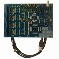
Manufacturer Part Number
CDB5376
Description
EVALUATION BOARD FOR CS5376
Manufacturer
Cirrus Logic Inc
Datasheets
1.CS5371A-ISZR.pdf
(32 pages)
2.CS4373A-ISZ.pdf
(34 pages)
3.CS5376A-IQZR.pdf
(106 pages)
4.CDB5378.pdf
(16 pages)
5.CDB5376.pdf
(80 pages)
6.CDB5376.pdf
(16 pages)
Specifications of CDB5376
Main Purpose
Seismic Evaluation System
Embedded
Yes, MCU, 8-Bit
Utilized Ic / Part
CS3301A, CS3302A, CS4373A, CS5372A, CS5376A
Primary Attributes
Quad Digital Filter
Secondary Attributes
Graphical User Interface, SPI™ & USB Interfaces
Processor To Be Evaluated
CS330x, CS4373A, CS537x
Interface Type
USB
Lead Free Status / RoHS Status
Contains lead / RoHS non-compliant
Lead Free Status / RoHS Status
Lead free / RoHS Compliant, Contains lead / RoHS non-compliant
Other names
598-1778


The CS5371A and CS5372A MSYNC input is
rising-edge triggered and resets the internal
MCLK counter/divider to guarantee synchro-
nous operation with other system devices.
While the MSYNC signal synchronizes the in-
ternal operation of the modulators, by default,
it does not synchronize the phase of the sine
wave from the CS4373A test DAC unless en-
abled in the digital filter TBSCFG register.
5.3 MDATA Connection
During normal operation the CS5371A and
CS5372A modulators output a ΔΣ serial bit
stream to the MDATA pin, with a one’s density
proportional to the differential amplitude of the
analog input signal. The output bit rate from
the MDATA output is a divide-by-four of the in-
put MCLK, and so is nominally 512 kHz.
The MDATA output has a 50% one’s density
for a mid-scale analog input, approximately
86% one’s density for a positive full-scale ana-
log input, and approximately 14% one’s densi-
ty for a negative full-scale analog input. One’s
density of the MDATA output is defined as the
ratio of ‘1’ bits to total bits in the serial bit
stream output; i.e. an 86% one’s density has,
on average, a ‘1’ value in 86 of every 100 out-
put data bits.
5.4 MFLAG Connection
The CS5371A and CS5372A ΔΣ modulators
have a fourth-order architecture which is con-
ditionally stable and may go into an oscillatory
condition if the analog inputs are over-ranged
more than 5% past either positive or negative
DS748F3
full-scale.
When an unstable condition is detected, the
modulator automatically collapses to a first-or-
der system to regain stability and then transi-
tions the MFLAG output low-to-high to signal
an error condition to the CS5376A digital filter.
The MFLAG output connects to a dedicated in-
put on the digital filter, causing an error flag to
be set in the status byte of the next output data
word.
For the modulator to recover from an unstable
condition, the analog input signal must be re-
duced to within the full-scale input range for at
least 32 MCLK cycles. If the analog input re-
mains over-ranged for an extended period, the
modulator will cycle between fourth-order and
first-order operation and the MFLAG output
will be seen to pulse.
5.5 OFST Connection
The CS5376A controls 12 general-purpose in-
put output (GPIO) pins through the digital filter
GPCFG register. These GPIO pins can be as-
signed to operate the CS5371A and CS5372A
OFST and PWDN pins.
If the OFST pin is pulled high, idle tones are
eliminated within the modulator by adding
-60 mV (channel 1 of CS5371A and CS5372A)
or -35 mV (channel 2 of CS5372A) of internal
differential offset during conversion to push
idle tones out of the measurement bandwidth.
Care should be taken to ensure external offset
voltages do not negate the internally added
differential offset, or idle tones will re-appear.
CS5371A CS5372A
19
Related parts for CDB5376
Image
Part Number
Description
Manufacturer
Datasheet
Request
R

Part Number:
Description:
Development Kit
Manufacturer:
Cirrus Logic Inc
Datasheet:
Part Number:
Description:
Development Kit
Manufacturer:
Cirrus Logic Inc
Datasheet:


Part Number:
Description:
High-efficiency PFC + Fluorescent Lamp Driver Reference Design
Manufacturer:
Cirrus Logic Inc
Datasheet:
Part Number:
Description:
Development Kit
Manufacturer:
Cirrus Logic Inc
Datasheet:
Part Number:
Description:
Development Kit
Manufacturer:
Cirrus Logic Inc
Datasheet:

Part Number:
Description:
Development Kit
Manufacturer:
Cirrus Logic Inc
Datasheet:
Part Number:
Description:
Development Kit
Manufacturer:
Cirrus Logic Inc
Datasheet:
Part Number:
Description:
Development Kit
Manufacturer:
Cirrus Logic Inc
Datasheet:
Part Number:
Description:
Development Kit
Manufacturer:
Cirrus Logic Inc
Datasheet:

Part Number:
Description:
EVALUATION BOARD FOR CS8427
Manufacturer:
Cirrus Logic Inc
Datasheet:

Part Number:
Description:
BOARD EVAL FOR CS8416 RCVR
Manufacturer:
Cirrus Logic Inc
Datasheet:

Part Number:
Description:
EVALUATION BOARD FOR CS8420
Manufacturer:
Cirrus Logic Inc
Datasheet:

Part Number:
Description:
KIT DEVELOPMENT EP9315 ARM9
Manufacturer:
Cirrus Logic Inc
Datasheet:

Part Number:
Description:
KIT DEVELOPMENT EP9302 ARM9
Manufacturer:
Cirrus Logic Inc
Datasheet: