CDB5376 Cirrus Logic Inc, CDB5376 Datasheet - Page 23
CDB5376
Manufacturer Part Number
CDB5376
Description
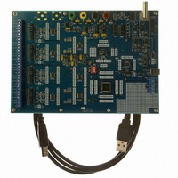
EVALUATION BOARD FOR CS5376
Manufacturer
Cirrus Logic Inc
Datasheets
1.CS5371A-ISZR.pdf
(32 pages)
2.CS4373A-ISZ.pdf
(34 pages)
3.CS5376A-IQZR.pdf
(106 pages)
4.CDB5378.pdf
(16 pages)
5.CDB5376.pdf
(80 pages)
6.CDB5376.pdf
(16 pages)
Specifications of CDB5376
Main Purpose
Seismic Evaluation System
Embedded
Yes, MCU, 8-Bit
Utilized Ic / Part
CS3301A, CS3302A, CS4373A, CS5372A, CS5376A
Primary Attributes
Quad Digital Filter
Secondary Attributes
Graphical User Interface, SPI™ & USB Interfaces
Processor To Be Evaluated
CS330x, CS4373A, CS537x
Interface Type
USB
Lead Free Status / RoHS Status
Contains lead / RoHS non-compliant
Lead Free Status / RoHS Status
Lead free / RoHS Compliant, Contains lead / RoHS non-compliant
Other names
598-1778


8. POWER SUPPLIES
The CS5371A and CS5372A modulators have
a positive analog power supply pin (VA+), a
negative analog power supply pin (VA-), a dig-
ital power supply pin (VD), and a ground pin
(GND).
For proper operation, power must be supplied
to all power supply pins, and the ground pin
must be connected to system ground. The
CS5371A and CS5372A digital power supply
(VD) and the CS5376A digital power supply
(VDD) must share a common voltage.
8.1 Power Supply Bypassing
The VA+, VA-, and VD power supplies should
be bypassed to system ground with 0.1 μF ca-
pacitors placed as close as possible to the
power pins of the device. In addition to the
0.1 μF local bypass capacitors, at least 100 μF
bulk capacitance to system ground should be
placed on each power supply near the voltage
regulator output, with additional power supply
bulk capacitance placed among the analog
component route if space permits. Bypass ca-
pacitors should be X7R, C0G, tantalum, or
other high-quality dielectric type.
8.2 PCB Layers and Routing
The CS5371A and CS5372A are high-perfor-
mance devices, and special care must be tak-
en to ensure power and ground routing is
correct. Power can be supplied either through
dedicated power planes or routed traces.
DS748F3
Regulator
To VA-
Regulator
100 uF
To VA+
100 uF
Figure 15. Power Supply Diagram
0.1 uF
0.1 uF
VA+
VA-
CS5371A
CS5372A
When routing power traces, it is recommended
to use a “star” routing scheme with the star
point either at the voltage regulator output or at
a local power supply bulk capacitor.
It is also recommended to dedicate a full PCB
layer to a solid ground plane, without splits or
routing. All bypass capacitors should connect
between the power supply circuit and the solid
ground plane as near as possible to the device
power supply pins.
The CS5371A and CS5372A analog signals
are differentially routed and do not normally re-
quire connection to a separate analog ground.
However, if a separate analog ground is re-
quired, it should be routed using a “star” rout-
ing scheme on a separate layer from the solid
ground plane and connected to the ground
plane only at a single point. Be sure all active
devices and passive components connected
to the separate analog ground are included in
the “star” route to ensure sensitive analog cur-
rents do not return through the ground plane.
8.3 Power Supply Rejection
Power supply rejection of the CS5371A and
CS5372A is frequency dependent. The
CS5376A digital filter fully rejects power sup-
ply noise for frequencies above the selected
digital filter corner frequency. Power supply
noise frequencies between DC and the digital
filter corner frequency are rejected as speci-
fied in the
GND
VD
Power Supply Characteristics
0.1 uF
CS5371A CS5372A
100 uF
Regulator
To VD
table.
23
Related parts for CDB5376
Image
Part Number
Description
Manufacturer
Datasheet
Request
R

Part Number:
Description:
Development Kit
Manufacturer:
Cirrus Logic Inc
Datasheet:
Part Number:
Description:
Development Kit
Manufacturer:
Cirrus Logic Inc
Datasheet:


Part Number:
Description:
High-efficiency PFC + Fluorescent Lamp Driver Reference Design
Manufacturer:
Cirrus Logic Inc
Datasheet:
Part Number:
Description:
Development Kit
Manufacturer:
Cirrus Logic Inc
Datasheet:
Part Number:
Description:
Development Kit
Manufacturer:
Cirrus Logic Inc
Datasheet:

Part Number:
Description:
Development Kit
Manufacturer:
Cirrus Logic Inc
Datasheet:
Part Number:
Description:
Development Kit
Manufacturer:
Cirrus Logic Inc
Datasheet:
Part Number:
Description:
Development Kit
Manufacturer:
Cirrus Logic Inc
Datasheet:
Part Number:
Description:
Development Kit
Manufacturer:
Cirrus Logic Inc
Datasheet:

Part Number:
Description:
EVALUATION BOARD FOR CS8427
Manufacturer:
Cirrus Logic Inc
Datasheet:

Part Number:
Description:
BOARD EVAL FOR CS8416 RCVR
Manufacturer:
Cirrus Logic Inc
Datasheet:

Part Number:
Description:
EVALUATION BOARD FOR CS8420
Manufacturer:
Cirrus Logic Inc
Datasheet:

Part Number:
Description:
KIT DEVELOPMENT EP9315 ARM9
Manufacturer:
Cirrus Logic Inc
Datasheet:

Part Number:
Description:
KIT DEVELOPMENT EP9302 ARM9
Manufacturer:
Cirrus Logic Inc
Datasheet: