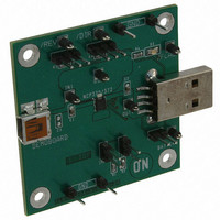
NCP370GEVB ON Semiconductor, NCP370GEVB Datasheet

EVAL BOARD FOR NCP370G

NCP370GEVB

Manufacturer Part Number
NCP370GEVB
Description
EVAL BOARD FOR NCP370G
Manufacturer
ON Semiconductor
Datasheets

Specifications of NCP370GEVB

Design Resources
NCP370GEVB BOM NCP370GEVB Gerber Files NCP370GEVB Schematic
Main Purpose
Overvoltage Protection
Embedded
No
Utilized Ic / Part
NCP370
Primary Attributes
Overvoltage Protected up to 28V and down to -28V
Secondary Attributes
Reverse Mode
Lead Free Status / RoHS Status
Lead free / RoHS Compliant
For Use With/related Products
NCP370G
Other names
NCP370GEVBOS
NCP370
Positive and Negative
Overvoltage Protection
with Internal Low R
N-MOSFETs and Reverse
Charge Control Pin
device. Two main modes are available by setting logic pins. First mode
is Direct Mode from Wall−Adapter to the system. In this mode the
system is both positive and negative over−voltage protected up to
+28 V and down to −28 V. The wall adapter (or AC/DC charger) is
disconnected from the system if the input voltage exceeds the
overvoltage (OVLO) or undervoltage (UVLO) thresholds. At power
up, the V
threshold.
allows an external accessory to be powered by the system battery or
boost converter. Here the external accessory would be connected to the
device input (bottom connector of system) and the device battery
would be at the device output. In this case overcurrent protection is
activated to prevent accessory faults and battery discharge. Thanks to
the NCP370 using an internal NMOS, the system cost and the PCB
area of the application board are minimized.
alerts the system that a fault has occurred.
bypassed with a 1 mF or larger capacitor.
Features
© Semiconductor Components Industries, LLC, 2010
August, 2010 − Rev. 5
The NCP370 is an overvoltage, overcurrent and reverse control
The second mode (see Tables 1 & 2), called the Reverse Mode,
The NCP370 provides a negative going flag (FLAG) output which
In addition, the device has ESD−protected input (15 kV Air) when
Alert FLAG Output
Compliance to IEC61000−4−2 (Level 4)
ESD Ratings: Machine Model = B
Human Body Model = 2
12 Lead TLLGA 3x3 mm Package
This is a Pb−Free Device
Overvoltage Protection Up to 28 V
Negative Voltage Protection Down to −28 V
Reverse Charge Control: REV
Direct Charge Control: DIR
Overcurrent Protection
Thermal Shutdown
On−chip Low R
Overvoltage Lockout (OVLO)
Undervoltage Lockout (UVLO)
Soft−Start
out
8 kV (Contact)
15 kV (Air)
turns on 30 ms after the V
DS(on)
NMOS Transistors: Typical 130 mW
in
exceeds the undervoltage
ON
1
Typical Applications
Cell Phones
Camera Phones
Digital Still Cameras
Personal Digital Applications
MP3 Players
†For information on tape and reel specifications,
NCP370MUAITXG
including part orientation and tape sizes, please
refer to our Tape and Reel Packaging Specification
Brochure, BRD8011/D.
CASE 513AK
12 PIN LLGA
GND
(Note: Microdot may be in either location)
RES
RES
RES
MU SUFFIX
Device
IN
IN
A
L
Y
W
G
1
ORDERING INFORMATION
1
2
3
4
5
6
http://onsemi.com
= Assembly Location
= Wafer Lot
= Year
= Work Week
= Pb−Free Package
(Pb−Free)
(Top View)
Package
LLGA12
NCP370
Publication Order Number:
MARKING
DIAGRAM
2500 / Tape &
ALYWG
NCAI
Shipping
10
12
370
11
9
8
7
G
Reel
NCP370/D
NC
OUT
FLAG
DIR
REV
Ilim

Related parts for NCP370GEVB

NCP370GEVB Summary of contents

Page 1

NCP370 Positive and Negative Overvoltage Protection with Internal Low R N-MOSFETs and Reverse Charge Control Pin The NCP370 is an overvoltage, overcurrent and reverse control device. Two main modes are available by setting logic pins. First mode is Direct Mode ...

Page 2

NCP370 Wall Adapter 1mF IN OUT 3 10 FLAG GND 4 9 RES DIR 8 5 RES REV 6 7 RES Ilim R limit INPUT DIR 10k Charger FLAG DIR REV 4.7mF GND Figure ...

Page 3

PIN FUNCTION DESCRIPTION Pin Name Type POWER Input voltage pins. These pins are connected to the power supply low ESR ceramic capacitor, or larger, must be connected between these pins and GND. The two ...

Page 4

ELECTRICAL CHARACTERISTICS values are +25°C) A Characteristics Symbols Input Voltage Range Input Voltage Vin Output Voltage Range Undervoltage Lockout Threshold UVLO Undervoltage Lockout Hysteresis UVLO Over voltage Lockout Threshold OVLO NCP370MUAITXG Overvoltage Lockout Hysteresis OVLO Over System ...

Page 5

... During overvoltage condition, the output is disabled as long as the input voltage exceeds OVLO. Additional OVLO thresholds can be manufactured (Please contact your ON Semiconductor representative for availability). FLAG output will be low since V This circuit has hysteresis to provide noise ...

Page 6

The FLAG pin goes low as soon the input voltage exceeds the OVLO threshold or falls below the UVLO threshold. When the V level recovers normal condition, FLAG goes in high after a time delay, t (see Figure 3), following ...

Page 7

V in ton rev V out FLAG DIR REV micro−controller Table 1. FLAG TABLE DIR REV 1.5 < V < UVLO > OVLO UVLO < V < OVLO ...

Page 8

Negative Voltage and Reverse Current. The device protects the downstream side from negative voltage occurring on the IN pin, down to −28 V. When a negative voltage occurs, the output is disconnected from the IN pins. Reverse Mode In Reverse ...

Page 9

At power up (accessory is plugged on input pins), the current is limited for 1.2 ms (typical), to allow lim capacitor charge and limit inrush current. If the I threshold is exceeded over 1.2 ms, the device ...

Page 10

ESD Tests The NCP370 conforms to the IEC61000−4−2, level 4 on the Input pin (I.E Murata GRM188R61E105KA12D) must be placed close to the IN pins. If the IEC61000−4−2 is not ...

Page 11

... 0.05 C NOTE 3 *For additional information on our Pb−Free strategy and soldering details, please download the ON Semiconductor Soldering and Mounting Techniques Reference Manual, SOLDERRM/D. N. American Technical Support: 800−282−9855 Toll Free USA/Canada Europe, Middle East and Africa Technical Support: Phone: 421 33 790 2910 Japan Customer Focus Center Phone: 81− ...

Related keywords