NCP370GEVB ON Semiconductor, NCP370GEVB Datasheet - Page 6
NCP370GEVB
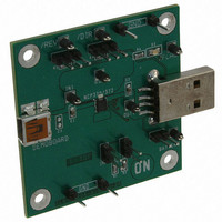
Manufacturer Part Number
NCP370GEVB
Description
EVAL BOARD FOR NCP370G
Manufacturer
ON Semiconductor
Specifications of NCP370GEVB
Design Resources
NCP370GEVB BOM NCP370GEVB Gerber Files NCP370GEVB Schematic
Main Purpose
Overvoltage Protection
Embedded
No
Utilized Ic / Part
NCP370
Primary Attributes
Overvoltage Protected up to 28V and down to -28V
Secondary Attributes
Reverse Mode
Lead Free Status / RoHS Status
Lead free / RoHS Compliant
For Use With/related Products
NCP370G
Other names
NCP370GEVBOS


the OVLO threshold or falls below the UVLO threshold.
When the V
high after a time delay, t
response. The FLAG pin is an open drain output and
disconnected from input, and FLAG pin goes low.
the micro−controller to appropriately process the
The FLAG pin goes low as soon the input voltage exceeds
During over thermal condition (T°
In Reverse Mode, FLAG pin remains available, allowing
FLAG
REV
V
DIR
in
V
out
in
level recovers normal condition, FLAG goes
start
t
on
(see Figure 3), following the V
t
start
Figure 3. FLAG Pin in AC/DC Charging Mode
J
>T°
t
t
stop
off
SD
), output is
http://onsemi.com
out
t
on
6
therefore a pull up resistor (typically 1 MW, minimum
10 kW) must be connected to Battery. The FLAG level will
always reflect V
= 1 and REV = 1).
overvoltage condition, overcurrent condition or thermal
shutdown condition.
t
start
t
dis
in
status, even if the device is turned off (DIR
> 1.2 V
OVLO
UVLO
Related parts for NCP370GEVB
Image
Part Number
Description
Manufacturer
Datasheet
Request
R

Part Number:
Description:
Positive and Negative Overvoltage Protection
Manufacturer:
ON Semiconductor
Datasheet:
Part Number:
Description:
ON Semiconductor [VOLTAGE REGULATOR]
Manufacturer:
ON Semiconductor
Datasheet:
Part Number:
Description:
357-036-542-201 CARDEDGE 36POS DL .156 BLK LOPRO
Manufacturer:
ON Semiconductor
Datasheet:
Part Number:
Description:
357-036-542-201 CARDEDGE 36POS DL .156 BLK LOPRO
Manufacturer:
ON Semiconductor
Datasheet:
Part Number:
Description:
357-036-542-201 CARDEDGE 36POS DL .156 BLK LOPRO
Manufacturer:
ON Semiconductor
Datasheet:
Part Number:
Description:
357-036-542-201 CARDEDGE 36POS DL .156 BLK LOPRO
Manufacturer:
ON Semiconductor
Datasheet:
Part Number:
Description:
357-036-542-201 CARDEDGE 36POS DL .156 BLK LOPRO
Manufacturer:
ON Semiconductor
Datasheet:
Part Number:
Description:
357-036-542-201 CARDEDGE 36POS DL .156 BLK LOPRO
Manufacturer:
ON Semiconductor
Datasheet:
Part Number:
Description:
357-036-542-201 CARDEDGE 36POS DL .156 BLK LOPRO
Manufacturer:
ON Semiconductor
Datasheet:
Part Number:
Description:
357-036-542-201 CARDEDGE 36POS DL .156 BLK LOPRO
Manufacturer:
ON Semiconductor
Datasheet:
Part Number:
Description:
357-036-542-201 CARDEDGE 36POS DL .156 BLK LOPRO
Manufacturer:
ON Semiconductor
Datasheet:
Part Number:
Description:
357-036-542-201 CARDEDGE 36POS DL .156 BLK LOPRO
Manufacturer:
ON Semiconductor
Datasheet:
Part Number:
Description:
Manufacturer:
ON Semiconductor
Datasheet:
Part Number:
Description:
Manufacturer:
ON Semiconductor
Datasheet: