DAK-16A Power Integrations, DAK-16A Datasheet - Page 9
DAK-16A
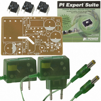
Manufacturer Part Number
DAK-16A
Description
KIT DESIGN ACCELERATOR ADAPTER
Manufacturer
Power Integrations
Series
LinkSwitch®r
Specifications of DAK-16A
Main Purpose
AC/DC, Primary Side
Outputs And Type
1, Isolated
Power - Output
2.75W
Voltage - Output
5.5V
Current - Output
500mA
Voltage - Input
85 ~ 265VAC
Regulator Topology
Flyback
Frequency - Switching
42kHz
Board Type
Bare (Unpopulated)
Utilized Ic / Part
LNK500, LNK501, LNK520
Lead Free Status / RoHS Status
Not applicable / Not applicable
Other names
596-1001


17-May-04
EPR-16 – LinkSwitch 2.75 W Charger/Adapter
4.2 LinkSwitch Operation
When power is applied to the supply, high voltage DC appears at the DRAIN pin of
LinkSwitch (U1). The CONTROL pin capacitor C3 is then charged through a switched
high voltage current source connected internally between the DRAIN and CONTROL
pins. When the CONTROL pin voltage reaches approximately 5.7 V relative to the
SOURCE pin, the internal current source is turned off. The internal control circuitry is
activated and the high voltage internal MOSFET starts to switch, using the energy in C3
to power the IC.
As the current ramps in the primary of flyback transformer T1, energy is stored. This
energy is delivered to the output when the MOSFET turns off each cycle.
The secondary of the transformer is rectified and filtered by D6 and C5 to provide the DC
output to the load.
Control of the output characteristic is entirely sensed from the primary-side by monitoring
the primary-side V
(voltage output reflected). While the output diode is conducting, the
OR
voltage across the transformer primary is equal to the output voltage plus diode drop
multiplied by the turns ratio of the transformer. Since the LinkSwitch is connected on the
high side of the transformer, the V
can be sensed directly.
OR
Diode D5 and capacitor C4 form the primary clamp network. The voltage held across C4
is essentially the V
with an error due to the parasitic leakage inductance.
OR
The LinkSwitch has three operating modes determined by the current flowing into the
CONTROL pin.
During start-up, as the output voltage, and therefore the reflected voltage and voltage
across C4 increases, the feedback current increases from 0 to approximately 2 mA
through R1 into the CONTROL pin. The internal current limit is increased during this
period until reaching 100%, providing an approximately constant output current.
Once the output voltage reaches the regulated CV value, the output voltage is regulated
through control of the duty cycle.
As the current into the CONTROL pin exceeds
approximately 2 mA, the duty cycle begins to reduce, reaching 30% at a CONTROL pin
current of 2.3 mA.
If the duty cycle reaches a 3% threshold, the switching frequency is reduced, which
reduces energy consumption under light or no load conditions.
As the output load increases beyond the peak power point (defined by ½·L·I²·f) and the
output voltage and V
falls, the reduced CONTROL pin current will lower the internal
OR
current providing an approximately constant current output characteristic. If the output
load is further increased and the output voltage falls further to below a CONTROL pin
current of 1 mA, the CONTROL pin capacitor C3 will discharge and the supply will enter
auto-restart.
Power Integrations
Page 9 of 36
Tel: +1 408 414 9660 Fax: +1 408 414 9760
www.powerint.com
Related parts for DAK-16A
Image
Part Number
Description
Manufacturer
Datasheet
Request
R

Part Number:
Description:
KIT REF DES DPA 6.6W DC-DC CONV
Manufacturer:
Power Integrations
Datasheet:

Part Number:
Description:
KIT DESIGN ACCELERATOR POE CONV
Manufacturer:
Power Integrations
Datasheet:

Part Number:
Description:
DESIGN ACCELERATOR KIT XT SWITCH
Manufacturer:
Power Integrations
Datasheet:

Part Number:
Description:
DESIGN ACCELERATOR KIT LP SWITCH
Manufacturer:
Power Integrations
Datasheet:

Part Number:
Description:
KIT DESIGN ACC PEAKSWITCH FAMILY
Manufacturer:
Power Integrations
Datasheet:

Part Number:
Description:
KIT DESIGN ACCELERATOR ADAPTER
Manufacturer:
Power Integrations
Datasheet:

Part Number:
Description:
KIT DESIGN ACCELERATOR DC-DC
Manufacturer:
Power Integrations
Datasheet:

Part Number:
Description:
KIT DESIGN ACCELERATOR DPA SW
Manufacturer:
Power Integrations
Datasheet:

Part Number:
Description:
KIT DESIGN ACCELERATOR AC/DC PS
Manufacturer:
Power Integrations
Datasheet:

Part Number:
Description:
KIT DESIGN ACCELERATOR MODEM
Manufacturer:
Power Integrations
Datasheet: