OM11055 NXP Semiconductors, OM11055 Datasheet
OM11055
Specifications of OM11055
Available stocks


Related parts for OM11055


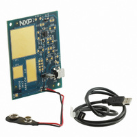
OM11055 Summary of contents
Page 1
PCF8883 Capacitive proximity switch with auto-calibration, large voltage operating range and very low power consumption Rev. 2 — 8 March 2011 1. General description The integrated circuit PCF8883 is a capacitive proximity switch that uses a patented (EDISEN) digital method ...
Page 2
... NXP Semiconductors 3. Applications Proximity detection Proximity sensing in Mobile phones Portable entertainment units Switch for medical applications Switch for use in explosive environments Vandal proof switches Transportation: Switches in or under upholstery, leather, handles, mats, and glass Buildings: switch in or under carpets, glass, or tiles Sanitary applications: use of standard metal sanitary parts (e ...
Page 3
... NXP Semiconductors 6. Block diagram IN (1) 150 nA. Fig 1. PCF8883 Product data sheet Capacitive proximity switch with auto-calibration V DD(INTREGD) V ref f s & & I sink V SS Block diagram of PCF8883 All information provided in this document is subject to legal disclaimers. Rev. 2 — 8 March 2011 V DD(INTREGD) V DD(INTREGD) VOLTAGE- ...
Page 4
... NXP Semiconductors 7. Pinning information 7.1 Pinning Fig 2. 7.2 Pin description Table 3. Symbol IN TYPE CPC OUT CLIN V DD(INTREGD) PCF8883 Product data sheet Capacitive proximity switch with auto-calibration 1 IN TYPE 2 PCF8883 3 CPC Top view. For mechanical details, see Pin configuration of PCF8883 (SOIC8) Pin description ...
Page 5
... NXP Semiconductors 8. Functional description Figure chip-internal RC timing circuit, to which the external sensing plate is connected dch via pin IN, is compared to the discharge time (t RC timing circuit. Both RC timing circuits are periodically charged from V identical switches and then discharged via a resistor to ground (V synchronized. ...
Page 6
... NXP Semiconductors If the capacitance on pin IN increases, the discharge time t will take longer for the voltage on the corresponding comparator to drop below V once this happens, the comparator output will become LOW and this results in a pulse on CDN discharging the external capacitor C by CUP. Without further action, capacitor C ...
Page 7
... NXP Semiconductors The counter, following the sensor logic depicted in CDN respectively. The counter is reset every time the pulse sequence changes from CUP to CDN or vice versa. Pin OUT will only be activated when a sufficient number of consecutive CUP or CDN pulses occur. Low level interference or slow changes in the input capacitance do not cause the output to switch ...
Page 8
... NXP Semiconductors Capacitance on input OUT (push-button) OUT (toggle) OUT · 2 ms/nF clk(H) TYPE (pulse) Fig 5. Switching modes timing diagram of PCF8883 8.2 Voltage regulator The PCF8883 implements a chip-internal voltage regulator supplied by pin V provides an internal supply (V voltage V V DD(INTREGD) maximum current of 0.5 mA). ...
Page 9
... NXP Semiconductors 9. Limiting values Table 4. In accordance with the Absolute Maximum Rating System (IEC 60134). Symbol Parameter tot V ESD stg T amb [1] Pass level; Human Body Model (HBM) according to [2] Pass level; Machine Model (MM), according to [3] Pass level; latch-up testing, according to [4] According to the NXP store and transport requirements (see stored at a temperature of +8 ° ...
Page 10
... NXP Semiconductors 10. Static characteristics Table 5. Static characteristics ° +25 C; unless otherwise specified. DD amb Symbol Parameter V supply voltage DD V lock-in voltage lockin V internal regulated supply voltage DD(INTREGD) ΔV internal regulated supply voltage DD(INTREGD) variation I supply current DD I sink current sink V output voltage ...
Page 11
... NXP Semiconductors 11. Dynamic characteristics Table 6. Dynamic characteristics pF 470 nF CLIN CPC Symbol Parameter C capacitance on pin CLIN CLIN C capacitance on pin CPC CPC N equivalent digital resolution res(dig)eq C capacitance on pin TYPE TYPE C input capacitance i R drain-source on-state resistance DSon t charge time ch t discharge time dch ...
Page 12
... NXP Semiconductors 12. Characteristic curves 12.1 Power consumption Fig 7. Fig 8. PCF8883 Product data sheet Capacitive proximity switch with auto-calibration 3 (μA) 3.0 2.5 2 °C. Idle state kHz amb I with respect 4 (μA) 3.5 3.0 2.5 2.0 1.5 −50 0 Idle state kHz with respect to temperature DD All information provided in this document is subject to legal disclaimers ...
Page 13
... NXP Semiconductors Fig 9. 12.2 Typical reaction time Fig 10. Switching time (t PCF8883 Product data sheet Capacitive proximity switch with auto-calibration 4 (μA) 3.5 3.0 2.5 2.0 1.5 250 750 = 25 °C. Idle state amb I with respect to sampling frequency (f DD 300 t sw (ms) 200 100 0 0 500 = 25 ° ...
Page 14
... NXP Semiconductors Fig 11. Switching time (t Fig 12. Switching time (t PCF8883 Product data sheet Capacitive proximity switch with auto-calibration 250 t sw (ms) 200 150 100 ° amb ) with respect to capacitor on pin CLIN ( (ms − with respect to temperature sw All information provided in this document is subject to legal disclaimers. ...
Page 15
... NXP Semiconductors 12.3 Reservoir capacitor voltage Fig 13. Input voltage on pin CPC (V Fig 14. Input voltage on pin CPC (V PCF8883 Product data sheet Capacitive proximity switch with auto-calibration 3 V I(CPC) ( ° amb V = input voltage on pin CPC. i(CPC capacitor on pin IN. IN i(CPC I(CPC) (V) 3.0 2 ...
Page 16
... NXP Semiconductors 13. Application information Figure 15 connected to pin V both V DD SENSING PLATE COAXIAL CABLE C SENS C = sensing plate capacitance. SENS The coaxial cable is optional. Fig 15. Typical application The sampling rate is determined by the capacitance C rate reduces the reaction time and increases the current consumption. ...
Page 17
... NXP Semiconductors interference. Pin CPC has a high-impedance and is sensitive to leakage currents. Therefore C type. When limiting the maximum input capacitance and the minimum operating temperature to −20 °C then the minimum operating voltage can be reduced to 2.8 V. The main limitation when lowering the supply voltage is a reduction in the range of the V voltage, which is specified from 0 ...
Page 18
... NXP Semiconductors 14. Package outline SOIC8: plastic small outline package; 8 leads; body width 3 pin 1 index 1 e Dimensions Unit max 1.73 0.25 1.48 mm nom min 1.37 0.10 1.27 max 0.068 0.0098 0.0582 inches nom min 0.054 0.0040 0.0500 Note 1. Plastic or metal protrusions of 0.15 mm (0.006 inch) maximum per side are not included. ...
Page 19
... NXP Semiconductors Fig 17. Three dimensional package drawing of PCF8883 (SOIC8) 15. Soldering of SMD packages This text provides a very brief insight into a complex technology. A more in-depth account of soldering ICs can be found in Application Note AN10365 “Surface mount reflow soldering description”. 15.1 Introduction to soldering Soldering is one of the most common methods through which packages are attached to Printed Circuit Boards (PCBs), to form electrical circuits ...
Page 20
... NXP Semiconductors 15.3 Wave soldering Key characteristics in wave soldering are: • Process issues, such as application of adhesive and flux, clinching of leads, board transport, the solder wave parameters, and the time during which components are exposed to the wave • Solder bath specifications, including temperature and impurities 15 ...
Page 21
... NXP Semiconductors Fig 18. Temperature profiles for large and small components For further information on temperature profiles, refer to Application Note AN10365 “Surface mount reflow soldering description”. 16. Abbreviations Table 9. Acronym CMOS HBM IC MM MOS MOSFET MSL PCB RC RF SMD PCF8883 Product data sheet ...
Page 22
... NXP Semiconductors 17. References [1] AN10365 — Surface mount reflow soldering description [2] AN10832 — PCF8883 - capacitive proximity switch with auto-calibration [3] IEC 60134 — Rating systems for electronic tubes and valves and analogous semiconductor devices [4] IEC 61340-5 — Protection of electronic devices from electrostatic phenomena [5] IPC/JEDEC J-STD-020D — ...
Page 23
... In no event shall NXP Semiconductors be liable for any indirect, incidental, punitive, special or consequential damages (including - without limitation - lost profits, lost savings, business interruption, costs related to the removal or ...
Page 24
... In the event that customer uses the product for design-in and use in automotive applications to automotive specifications and standards, customer (a) shall use the product without NXP Semiconductors’ warranty of the product for such automotive applications, use and specifications, and (b) whenever customer uses the product for automotive applications beyond NXP Semiconductors’ ...
Page 25
... NXP Semiconductors 21. Contents 1 General description . . . . . . . . . . . . . . . . . . . . . . 1 2 Features and benefits . . . . . . . . . . . . . . . . . . . . 1 3 Applications . . . . . . . . . . . . . . . . . . . . . . . . . . . . 2 4 Ordering information . . . . . . . . . . . . . . . . . . . . . 2 5 Marking . . . . . . . . . . . . . . . . . . . . . . . . . . . . . . . . 2 6 Block diagram . . . . . . . . . . . . . . . . . . . . . . . . . . 3 7 Pinning information . . . . . . . . . . . . . . . . . . . . . . 4 7.1 Pinning . . . . . . . . . . . . . . . . . . . . . . . . . . . . . . . 4 7.2 Pin description . . . . . . . . . . . . . . . . . . . . . . . . . 4 8 Functional description . . . . . . . . . . . . . . . . . . . 5 8.1 Output switching modes . . . . . . . . . . . . . . . . . . 7 8.2 Voltage regulator Limiting values Static characteristics Dynamic characteristics ...