OM11055 NXP Semiconductors, OM11055 Datasheet - Page 7
OM11055
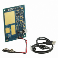
Manufacturer Part Number
OM11055
Description
EVAL BOARD FOR PCF8883
Manufacturer
NXP Semiconductors
Specifications of OM11055
Sensor Type
Capacitive
Interface
Mini USB
Voltage - Supply
3 V ~ 9 V
Embedded
No
Utilized Ic / Part
PCF8883
Lead Free Status / RoHS Status
Lead free / RoHS Compliant
Sensitivity
-
Sensing Range
-
Other names
568-4958
Available stocks
Company
Part Number
Manufacturer
Quantity
Price
Company:

Part Number:
OM11055
Manufacturer:
NXP Semiconductors
Quantity:
135
Company:
Part Number:
OM11055598
Manufacturer:
NXP Semiconductors
Quantity:
135


NXP Semiconductors
2.
PCF8883
Product data sheet
A capacitive event is a dynamic increase of capacitance at the sensor input pin IN.
8.1 Output switching modes
The counter, following the sensor logic depicted in
CDN respectively. The counter is reset every time the pulse sequence changes from CUP
to CDN or vice versa. Pin OUT will only be activated when a sufficient number of
consecutive CUP or CDN pulses occur. Low level interference or slow changes in the
input capacitance do not cause the output to switch.
Various measures, such as asymmetrical charge and discharge steps, are taken to
ensure that the output switches off correctly. A special start-up circuit ensures that the
device reaches equilibrium quickly when the supply is attached.
Pin OUT is an open-drain output capable of pulling an external load R
current of 20 mA) up to V
the maximum expected V
deactivated (short circuit protection) for loads in excess of 30 mA. Pin OUT can also drive
a CMOS input without connection of the external load.
A small internal 150 nA current sink I
OUT, even if no load resistor is connected. This is useful for driving purely capacitive
CMOS inputs. The falling slope can be fairly slow in this mode, depending on load
capacitance.
The sampling rate (f
The sampling rate can be adjusted within a specified range by selecting the value of
C
signal. This prevents interference caused by local AC-fields.
The output switching behavior can be selected using pin TYPE (see
A typical value for C
10 ms. The maximum value of C
about 1 s. Capacitive events are ignored that occur during the time the output is active.
Figure 5
graph illustrates, that short term disturbances on the sensor are suppressed by the circuit.
CLIN
•
•
•
Push-button (TYPE connected to V
capacitive event
Toggle (TYPE connected to V
capacitive event and deactivated by a following capacitive event.
Pulse (C
defined time at each capacitive event. The pulse duration is determined by the value
of C
. The oscillator frequency is internally modulated by 4 % using a pseudo random
TYPE
illustrates the switching behavior for the output switching modes. Additionally the
TYPE
and is approximately 2.5 ms/nF.
All information provided in this document is subject to legal disclaimers.
connected between TYPE and V
s
TYPE
2
) corresponds to half of the frequency used in the RC timing circuit.
lasts.
Rev. 2 — 8 March 2011
is 4.7 nF which results in an output pulse duration of about
DD
DD
. The load resistor must be dimensioned appropriately, taking
voltage into account. The output will be automatically
TYPE
DD(INTREGD)
sink
Capacitive proximity switch with auto-calibration
is 470 nF which results in a pulse duration of
SS
enables a full voltage swing to take place on
): The output OUT is active as long as the
): The output OUT is activated by the first
SS
Figure
): The output OUT is activated for a
3, counts the pulses of CUP or
Figure
ext
PCF8883
© NXP B.V. 2011. All rights reserved.
(at maximum
5)
7 of 25
Related parts for OM11055
Image
Part Number
Description
Manufacturer
Datasheet
Request
R

Part Number:
Description:
NXP Semiconductors designed the LPC2420/2460 microcontroller around a 16-bit/32-bitARM7TDMI-S CPU core with real-time debug interfaces that include both JTAG andembedded trace
Manufacturer:
NXP Semiconductors
Datasheet:

Part Number:
Description:
NXP Semiconductors designed the LPC2458 microcontroller around a 16-bit/32-bitARM7TDMI-S CPU core with real-time debug interfaces that include both JTAG andembedded trace
Manufacturer:
NXP Semiconductors
Datasheet:
Part Number:
Description:
NXP Semiconductors designed the LPC2468 microcontroller around a 16-bit/32-bitARM7TDMI-S CPU core with real-time debug interfaces that include both JTAG andembedded trace
Manufacturer:
NXP Semiconductors
Datasheet:
Part Number:
Description:
NXP Semiconductors designed the LPC2470 microcontroller, powered by theARM7TDMI-S core, to be a highly integrated microcontroller for a wide range ofapplications that require advanced communications and high quality graphic displays
Manufacturer:
NXP Semiconductors
Datasheet:
Part Number:
Description:
NXP Semiconductors designed the LPC2478 microcontroller, powered by theARM7TDMI-S core, to be a highly integrated microcontroller for a wide range ofapplications that require advanced communications and high quality graphic displays
Manufacturer:
NXP Semiconductors
Datasheet:
Part Number:
Description:
The Philips Semiconductors XA (eXtended Architecture) family of 16-bit single-chip microcontrollers is powerful enough to easily handle the requirements of high performance embedded applications, yet inexpensive enough to compete in the market for hi
Manufacturer:
NXP Semiconductors
Datasheet:
Part Number:
Description:
The XA-S3 device is a member of Philips Semiconductors? XA(eXtended Architecture) family of high performance 16-bitsingle-chip microcontrollers
Manufacturer:
NXP Semiconductors
Datasheet:

Part Number:
Description:
The NXP BlueStreak LH75401/LH75411 family consists of two low-cost 16/32-bit System-on-Chip (SoC) devices
Manufacturer:
NXP Semiconductors
Datasheet:
Part Number:
Description:
The NXP LPC3130/3131 combine an 180 MHz ARM926EJ-S CPU core, high-speed USB2
Manufacturer:
NXP Semiconductors
Datasheet:
Part Number:
Description:
The NXP LPC3141 combine a 270 MHz ARM926EJ-S CPU core, High-speed USB 2
Manufacturer:
NXP Semiconductors
Part Number:
Description:
The NXP LPC3143 combine a 270 MHz ARM926EJ-S CPU core, High-speed USB 2
Manufacturer:
NXP Semiconductors

Part Number:
Description:
The NXP LPC3152 combines an 180 MHz ARM926EJ-S CPU core, High-speed USB 2
Manufacturer:
NXP Semiconductors
Part Number:
Description:
The NXP LPC3154 combines an 180 MHz ARM926EJ-S CPU core, High-speed USB 2
Manufacturer:
NXP Semiconductors

Part Number:
Description:
Standard level N-channel enhancement mode Field-Effect Transistor (FET) in a plastic package using NXP High-Performance Automotive (HPA) TrenchMOS technology
Manufacturer:
NXP Semiconductors
Datasheet: