ADIS16365/PCBZ Analog Devices Inc, ADIS16365/PCBZ Datasheet - Page 11
ADIS16365/PCBZ
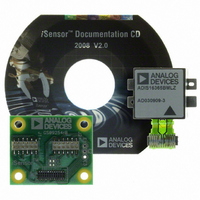
Manufacturer Part Number
ADIS16365/PCBZ
Description
BOARD INTERFACE FOR ADIS16365
Manufacturer
Analog Devices Inc
Series
iMEMS®, iSensor™r
Specifications of ADIS16365/PCBZ
Sensor Type
Accelerometer, Gyroscope, 3 Axis
Sensing Range
±17g, ±75°/sec, ±150°/sec, ±300°/sec
Interface
SPI Serial
Sensitivity
3.3mg/LSB, 0.0125 ~ 0.05°/sec/LSB
Voltage - Supply
4.75 V ~ 5.25 V
Embedded
No
Utilized Ic / Part
ADIS16365
Silicon Manufacturer
Analog Devices
Application Sub Type
Accelerometer / Gyroscope
Kit Application Type
Sensing - Motion / Vibration / Shock
Silicon Core Number
ADIS16365
Lead Free Status / RoHS Status
Not applicable / RoHS Compliant
For Use With
ADISUSBZ - KIT EVAL ADIS W/SOFTWARE USB
Lead Free Status / RoHS Status
Lead free / RoHS Compliant, Not applicable / RoHS Compliant


BURST READ DATA COLLECTION
Burst read data collection is a process-efficient method for
collecting data from the ADIS16360/ADIS16365. In a burst
read, all output data registers are clocked out on DOUT, 16 bits
at a time, in sequential data cycles (each separated by one SCLK
period). To start a burst read sequence, set DIN = 0x3E00. The
contents of each output data register are then shifted out on
DOUT, starting with SUPPLY_OUT and ending with AUX_ADC
(see Figure 13) in order by address (see Table 8).
OUTPUT DATA REGISTERS
Each output data register uses the format in Figure 12 and Table 9.
Figure 6 shows the positive direction for each inertial sensor. The
ND bit is equal to 1 when the register contains unread data. The
EA bit is high when any error/alarm flag in the DIAG_STAT
register is equal to 1.
Table 9. Output Data Register Formats
Register
SUPPLY_OUT
XGYRO_OUT
YGYRO_OUT
ZGYRO_OUT
XACCL_OUT
YACCL_OUT
ZACCL_OUT
XTEMP_OUT
YTEMP_OUT
ZTEMP_OUT
AUX_ADC
1
2
Table 10. Power Supply, Offset Binary Format
Supply Voltage
5.25 V
5.002418 V
5 V
4.997582 V
4.75 V
Assumes that the scaling is set to ±300°/sec. This factor scales with the range.
0x0000 = 25°C (±5°C).
DOUT
NOTES
1. THE DOUT LINE HAS BEEN SIMPLIFIED FOR SPACE CONSTRAINTS BUT, IDEALLY, SHOULD INCLUDE ALL REGISTERS FROM SUPPLY_OUT THROUGH AUX_ADC.
ND EA
SCLK
DIN
CS
Figure 12. Output Data Register Bit Assignments
1
2
2
2
1
1
PREVIOUS
0x3E00
Bits
12
14
14
14
14
14
14
12
12
12
12
Decimal
2171 LSB
2069 LSB
2068 LSB
2067 LSB
1964 LSB
1
MSB FOR 14-BIT OUTPUT
Hex
0x87B
0x815
0x814
0x813
0x7AC
Scale
2.418 mV
0.05°/sec
0.05°/sec
0.05°/sec
3.333 mg
3.333 mg
3.333 mg
0.136°C
0.136°C
0.136°C
805.8 μV
MSB FOR 12-BIT OUTPUT
SUPPLY_OUT
DON’T CARE
2
Binary
XXXX 1000 0111 1011
XXXX 1000 0001 0101
XXXX 1000 0001 0100
XXXX 1000 0001 0011
XXXX 0111 1010 1100
Reference
See Table 10
See Table 11
See Table 11
See Table 11
See Table 12
See Table 12
See Table 12
See Table 13
See Table 13
See Table 13
See Table 14
XGYRO_OUT
3
Figure 13. Burst Read Sequence
Rev. D | Page 11 of 20
YGYRO_OUT
4
Table 11. Rotation Rate, Twos Complement Format
Rotation Rate
+300°/sec
+0.1°/sec
+0.05°/sec
0°/sec
−0.05°/sec
−0.1°/sec
−300°/sec
Table 12. Acceleration, Twos Complement Format
Acceleration
+18 g
+6.667 mg
+3.333 mg
0 g
−3.333 mg
−6.667 mg
−18 g
Table 13. Temperature, Twos Complement Format
Temperature
+105°C
+85°C
+25.272°C
+25.136°C
+25°C
+24.864°C
+24.728°C
−40°C
Table 14. Analog Input, Offset Binary Format
Input Voltage
3.3 V
1 V
1.6116 mV
805.8 μV
0 V
ZGYRO_OUT
5
Decimal
+6000 LSB
+2 LSB
+1 LSB
0 LSB
−1 LSB
−2 LSB
−6000 LSB
Decimal
+5401 LSB
+2 LSB
+1 LSB
0 LSB
−1 LSB
−2 LSB
−5401 LSB
Decimal
+588 LSB
+441 LSB
+2 LSB
+1 LSB
0 LSB
−1 LSB
−2 LSB
−478 LSB
Decimal
4095 LSB
1241 LSB
2 LSB
1 LSB
0 LSB
AUX_ADC
ADIS16360/ADIS16365
12
Hex
0x1770
0x0002
0x0001
0x0000
0x3FFF
0x3FFE
0x2890
Hex
0x1519
0x0002
0x0001
0x0000
0x3FFF
0x3FFE
0x2AE7
Hex
0x24C
0x1B9
0x002
0x001
0x000
0xFFF
0xFFE
0xE22
Hex
0xFFF
0x4D9
0x002
0x001
0x000
Binary
XX01 0111 0111 0000
XX00 0000 0000 0010
XX00 0000 0000 0001
XX00 0000 0000 0000
XX11 1111 1111 1111
XX11 1111 1111 1110
XX10 1000 1001 0000
Binary
XX01 0101 0001 1001
XX00 0000 0000 0010
XX00 0000 0000 0001
XX00 0000 0000 0000
XX11 1111 1111 1111
XX11 1111 1111 1110
XX10 1010 1110 0111
Binary
XXXX 0010 0100 1100
XXXX 0001 1011 1001
XXXX 0000 0000 0010
XXXX 0000 0000 0001
XXXX 0000 0000 0000
XXXX 1111 1111 1111
XXXX 1111 1111 1110
XXXX 1110 0010 0010
Binary
XXXX 1111 1111 1111
XXXX 0100 1101 1001
XXXX 0000 0000 0010
XXXX 0000 0000 0001
XXXX 0000 0000 0000
Related parts for ADIS16365/PCBZ
Image
Part Number
Description
Manufacturer
Datasheet
Request
R

Part Number:
Description:
±1.7g Dual-Axis IMEMS Accelerometer Evaluation Board
Manufacturer:
Analog Devices Inc
Datasheet:

Part Number:
Description:
Inertial Sensor Evaluation System
Manufacturer:
Analog Devices Inc
Datasheet:
Part Number:
Description:
Manufacturer:
Analog Devices Inc
Datasheet:
Part Number:
Description:
Manufacturer:
Analog Devices Inc
Datasheet:
Part Number:
Description:
Manufacturer:
Analog Devices Inc
Datasheet:
Part Number:
Description:
Manufacturer:
Analog Devices Inc
Datasheet:
Part Number:
Description:
Manufacturer:
Analog Devices Inc
Datasheet:
Part Number:
Description:
Manufacturer:
Analog Devices Inc
Datasheet:
Part Number:
Description:
Manufacturer:
Analog Devices Inc
Datasheet:
Part Number:
Description:
Manufacturer:
Analog Devices Inc
Datasheet:
Part Number:
Description:
Manufacturer:
Analog Devices Inc
Datasheet:
Part Number:
Description:
Manufacturer:
Analog Devices Inc
Datasheet:
Part Number:
Description:
Manufacturer:
Analog Devices Inc
Datasheet: