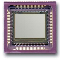
CYII5SC1300-EVAL Cypress Semiconductor Corp, CYII5SC1300-EVAL Datasheet - Page 4

CYII5SC1300-EVAL
Manufacturer Part Number
CYII5SC1300-EVAL
Description
BOARD EVAL IMG SENS IBIS5-B-1300
Manufacturer
Cypress Semiconductor Corp
Specifications of CYII5SC1300-EVAL
Sensor Type
CMOS Imaging, Color (RGB)
Sensing Range
1.3 Megapixel
Interface
Parallel/Serial
Sensitivity
106 fps
Voltage - Supply
3 V ~ 4.5 V
Embedded
No
Utilized Ic / Part
IBIS5-B-1300
Lead Free Status / RoHS Status
Contains lead / RoHS non-compliant
Lead Free Status / RoHS Status
Lead free / RoHS Compliant, Contains lead / RoHS non-compliant
Document #: 38-05710 Rev. *A
RBT: Row Blanking Time = 3.5 ms (typical).
Pixel period: 1/40 MHz = 25 ns.
Example Read out time of the full resolution at nominal speed
(40 MHz pixel rate) with an integration time of 1 ms:
37.4 ms
Region-Of-Interest (ROI) Read Out
Windowing can easily be achieved by uploading the starting
point of the x- and y-shift registers in the sensor registers using
the various interfaces. This downloaded starting point initiates
the shift register in the x- and y-direction triggered by the
Y_START (initiates the Y-shift register) and the Y_CLK
(initiates the X-shift register) pulse. The minimum step size for
the x-address is 2 (only even start addresses can be chosen)
and 1 for the Y-address (every line can be addressed). The
frame rate increases almost linearly when fewer pixels are
read out.
rates (in rolling shutter mode) with various ROI dimensions.
Table 2. Frame Rate vs. Resolution
=> Frame period = 1 ms + (1024 * (3.5 ms + 25 ns * 1280)) =
1280 x 1024
Resolution
640 x 480
100 x 100
Image
(X*Y)
Table 2
=> 26.8 fps.
VDDR_LEFT
SYS_CLOCK
Frame Rate
[frames/s]
gives an overview of the achievable frame
Y_CLOCK
Y_START
VDDH
1657
Y-left addressing
100
27
Readout Time
BUS_A
BUS_B
Frame
[ms]
Read-pointer
0.6
36
10
Pixel column
Full resolution.
ROI read out.
ROI read out.
Comment
Figure 5. Image Core
X addressing
Pixel
SAMPLE
A
RESET
HOLD
Pixel
B
Image Core Operation
Image Core Operation and Signalling
Figure 5
without sub-sampling and column/row swapping circuits. Most
of the involved signals are not available from the outside
because they are generated by the X-sequencer and
SS-sequencer blocks.
The integration of the pixels is controlled by internal signals
such as reset, sample, hold are generated by the on-chip
SS-sequencer that is controlled with the external signals
SS_START and SS_STOP. Reading out the pixel array starts
by applying a Y_START together with a Y_CLOCK signal;
internally this is followed by a calibration sequence to calibrate
the output amplifiers (during the row blanking time); signals
necessary to do this calibration are generated by the on-chip
X-sequencer. This calibration sequence takes typically 3.5 µ s
and is necessary to remove Fixed Pattern Noise of the pixels
and of the column amplifiers themselves by means of a Double
Sampling technique. After the row blanking time the pixels are
fed to the output amplifier. The pixel rate is equal to the
SYS_CLOCK frequency.
Image Core Supply Considerations
The image sensor has several supply voltages:
VDDH is the voltage that controls the sample switches and
must always be the highest voltage that is applied to the chip.
The VDDR_LEFT voltage is the highest (nominal) reset
voltage of the pixel core.
Pixel row
Column amplifiers
is a functional representation of the image core
Output amplifier
Y-right addressing
Y_START
Y_CLOCK
PXL_OUT
Vddreset
VDDR_RIGHT
VDDC
CYII5FM1300AB
IBIS5-B-1300
Page 4 of 42
[+] Feedback


