CYII5SC1300-EVAL Cypress Semiconductor Corp, CYII5SC1300-EVAL Datasheet - Page 5
CYII5SC1300-EVAL
Manufacturer Part Number
CYII5SC1300-EVAL
Description
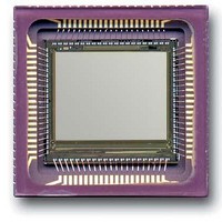
BOARD EVAL IMG SENS IBIS5-B-1300
Manufacturer
Cypress Semiconductor Corp
Specifications of CYII5SC1300-EVAL
Sensor Type
CMOS Imaging, Color (RGB)
Sensing Range
1.3 Megapixel
Interface
Parallel/Serial
Sensitivity
106 fps
Voltage - Supply
3 V ~ 4.5 V
Embedded
No
Utilized Ic / Part
IBIS5-B-1300
Lead Free Status / RoHS Status
Contains lead / RoHS non-compliant
Lead Free Status / RoHS Status
Lead free / RoHS Compliant, Contains lead / RoHS non-compliant


Document #: 38-05710 Rev. *A
The
VDDR_LEFT voltage using a circuit that can be programmed
with the KNEEPOINT_LSB/MSB bits in the sequencer register
(see also
(bits 8, 9, and 10).” on page
VDDR_RIGHT_EXT bit in the SEQUENCER register, the
VDDR_RIGHT pin can be disconnected from the circuit and
an external voltage can be applied to supply the multiple slope
reset voltage. When no external voltage is applied (recom-
mended) the VDDR_RIGHT pin should be connected to a
capacitor (recommended value = 1µF). VDDC is the supply of
the pixel core. VDDA is the analog supply of the image core
and periphery. VDDD is the digital supply of the image core
and periphery.
Note that the IBIS5-B-1300 image sensor has no power
rejection circuitry on-chip. As a consequence all variations on
the analog supply voltages can contribute to random variations
(noise) on the analog pixel signal, which is seen as random
noise in the image. During the camera design precautions
have to be taken to supply the sensor with very stable supply
voltages to avoid this additional noise. Especially the analog
supplies of the pixel array (VDDR_LEFT, VDDH and VDDC)
are vulnerable for this.
Snapshot Shutter Supply Considerations
When using the IBIS5-B-1300 sensor in snapshot shutter
mode only the recommended supply voltage settings are listed
below in
Table 3. Snapshot Shutter Recommended Supply
Settings
Table 5. Overview of Bias Signals
DEC_CMD
DAC_VHIGH Connect to VDDA with R = 0 Ω .
DAC_VLOW Connect to GNDA with R = 0 Ω .
AMP_CMD
COL_CMD
PC_CMD
ADC_CMD
ADC_VHIGH Connect to VDDA with R = 360 Ω and decouple to GNDA with C = 100 nF. High level of ADC.
ADC_VLOW Connect to GNDA with R = 1200 Ω and decouple to GNDA with C = 100 nF. Low level of ADC.
VDDH
VDDR_LEFT Highest reset voltage.
VDDC
VDDA
VDDD
GNDA
GNDD
GND_AB
Parameter
Signal
VDDR_RIGHT
Table
“Pixel Reset Knee-point for Multiple Slope Operation
Voltage on HOLD switches.
Pixel core voltage.
Analog supply voltage of the
image core.
Digital supply voltage of the
image core.
Analog ground.
Digital ground.
Anti-blooming ground.
3.
Connect to VDDA with R = 50 k Ω and decouple to GNDA with C = 100 nF. Decoder stage.
Connect to VDDA with R = 50 k Ω and decouple to GNDA with C = 100 nF. Output amplifier stage.
Connect to VDDA with R = 50 k Ω and decouple to GNDA with C = 100 nF. Columns amplifiers stage.
Connect to VDDA with R = 25 k Ω and decouple to GNDA with C = 100 nF. Pre-charge of column
Connect to VDDA with R = 50 k Ω and decouple to GNDA with C = 100 nF. Analog stage of ADC.
Description
voltage
is
generated
14). By setting the
Typ.
+3.3
+3.3
+3.3
+4.5
+4.5
Comment
0
0
0
from
Unit
V
V
V
V
V
V
V
V
the
Dual Shutter Supply Considerations
With the supply settings listed in
non-uniformities (FPN) can be seen when operating in rolling
shutter mode. If a dual shutter mode (both rolling and snapshot
shutter) is required during operation one needs to apply the
supply settings listed in
possible image quality.
Table 4. Dual Shutter Recommended Supply Settings
Image Core Biasing Signals
Table 5
IBIS5-A-1300. For optimizations reasons with respect to
speed and power dissipation of all internal block several
biasing resistors are needed.
Each biasing signal determines the operation of a corre-
sponding module in the sense that it controls the speed and
power dissipation. The tolerance on the DC-level of the bias
levels can vary ±150 mV due to process variations.
VDDH
VDDR_LEFT Highest reset voltage.
VDDC
VDDA
VDDD
GNDA
GNDD
GND_AB
Parameter
summarizes the biasing signals required to drive the
Voltage on HOLD switches.
Pixel core voltage.
Analog supply voltage of the
image core.
Digital supply voltage of the
image core.
Analog ground.
Digital ground.
Anti-blooming ground.
High level of DAC.
Low level of DAC.
busses.
Description
Table 4
Related module
CYII5FM1300AB
Table 3
below to achieve the best
IBIS5-B-1300
some fixed column
Page 5 of 42
Typ. Unit
+4.5
+4.5
+3.0
+3.3
+3.3
DC-level
0
0
0
1.0V
1.8V
1.0V
3.3V
0.0V
1.2V
1.0V
1.1V
2.7V
V
V
V
V
V
V
V
V
[+] Feedback
Related parts for CYII5SC1300-EVAL
Image
Part Number
Description
Manufacturer
Datasheet
Request
R

Part Number:
Description:
Manufacturer:
Cypress Semiconductor Corp
Datasheet:
Part Number:
Description:
Manufacturer:
Cypress Semiconductor Corp
Datasheet:
Part Number:
Description:
Manufacturer:
Cypress Semiconductor Corp
Datasheet:
Part Number:
Description:
Manufacturer:
Cypress Semiconductor Corp
Datasheet:
Part Number:
Description:
Manufacturer:
Cypress Semiconductor Corp
Datasheet: