C8051F320DK Silicon Laboratories Inc, C8051F320DK Datasheet - Page 24
C8051F320DK
Manufacturer Part Number
C8051F320DK
Description
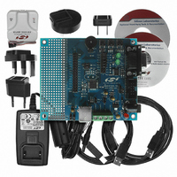
DEV KIT FOR C8051F320/F321
Manufacturer
Silicon Laboratories Inc
Type
MCUr
Specifications of C8051F320DK
Contents
Evaluation Board, Power Supply, USB Cables, Adapter and Documentation
Processor To Be Evaluated
C8051F320/F321
Interface Type
USB
Silicon Manufacturer
Silicon Labs
Core Architecture
8051
Silicon Core Number
C8051F320
Silicon Family Name
C8051F32x
Lead Free Status / RoHS Status
Contains lead / RoHS non-compliant
For Use With/related Products
Silicon Laboratories C8051F320, C8051F321
Lead Free Status / Rohs Status
Lead free / RoHS Compliant
Other names
336-1260
Available stocks
Company
Part Number
Manufacturer
Quantity
Price
Company:

Part Number:
C8051F320DK
Manufacturer:
SiliconL
Quantity:
4


C8051F320/1
1.9.
The C8051F320/1 devices include an on-chip 10-bit SAR ADC with a 17-channel differential input multi-
plexer. With a maximum throughput of 200 ksps, the ADC offers true 10-bit linearity with an INL of ±1LSB.
The ADC system includes a configurable analog multiplexer that selects both positive and negative ADC
inputs. Ports1-3 are available as ADC inputs; additionally, the on-chip Temperature Sensor output and the
power supply voltage (VDD) are available as ADC inputs. User firmware may shut down the ADC to save
power.
Conversions can be started in six ways: a software command, an overflow of Timer 0, 1, 2, or 3, or an
external convert start signal. This flexibility allows the start of conversion to be triggered by software
events, a periodic signal (timer overflows), or external HW signals. Conversion completions are indicated
by a status bit and an interrupt (if enabled). The resulting 10-bit data word is latched into the ADC data
SFRs upon completion of a conversion.
Window compare registers for the ADC data can be configured to interrupt the controller when ADC data is
either within or outside of a specified range. The ADC can monitor a key voltage continuously in back-
ground mode, but not interrupt the controller unless the converted data is within/outside the specified
range.
24
10-Bit Analog to Digital Converter
Capture/Compare
Module 0
SYSCLK/12
SYSCLK/4
Timer 0 Overflow
SYSCLK
External Clock/8
ECI
Figure 1.9. PCA Block Diagram
Capture/Compare
Module 1
CLOCK
MUX
PCA
Crossbar
16-Bit Counter/Timer
Port I/O
Rev. 1.4
Capture/Compare
Module 2
Capture/Compare
Module 3
Capture/Compare
Module 4 / WDT
Related parts for C8051F320DK
Image
Part Number
Description
Manufacturer
Datasheet
Request
R

Part Number:
Description:
SMD/C°/SINGLE-ENDED OUTPUT SILICON OSCILLATOR
Manufacturer:
Silicon Laboratories Inc
Part Number:
Description:
Manufacturer:
Silicon Laboratories Inc
Datasheet:
Part Number:
Description:
N/A N/A/SI4010 AES KEYFOB DEMO WITH LCD RX
Manufacturer:
Silicon Laboratories Inc
Datasheet:
Part Number:
Description:
N/A N/A/SI4010 SIMPLIFIED KEY FOB DEMO WITH LED RX
Manufacturer:
Silicon Laboratories Inc
Datasheet:
Part Number:
Description:
N/A/-40 TO 85 OC/EZLINK MODULE; F930/4432 HIGH BAND (REV E/B1)
Manufacturer:
Silicon Laboratories Inc
Part Number:
Description:
EZLink Module; F930/4432 Low Band (rev e/B1)
Manufacturer:
Silicon Laboratories Inc
Part Number:
Description:
I°/4460 10 DBM RADIO TEST CARD 434 MHZ
Manufacturer:
Silicon Laboratories Inc
Part Number:
Description:
I°/4461 14 DBM RADIO TEST CARD 868 MHZ
Manufacturer:
Silicon Laboratories Inc
Part Number:
Description:
I°/4463 20 DBM RFSWITCH RADIO TEST CARD 460 MHZ
Manufacturer:
Silicon Laboratories Inc
Part Number:
Description:
I°/4463 20 DBM RADIO TEST CARD 868 MHZ
Manufacturer:
Silicon Laboratories Inc
Part Number:
Description:
I°/4463 27 DBM RADIO TEST CARD 868 MHZ
Manufacturer:
Silicon Laboratories Inc
Part Number:
Description:
I°/4463 SKYWORKS 30 DBM RADIO TEST CARD 915 MHZ
Manufacturer:
Silicon Laboratories Inc
Part Number:
Description:
N/A N/A/-40 TO 85 OC/4463 RFMD 30 DBM RADIO TEST CARD 915 MHZ
Manufacturer:
Silicon Laboratories Inc
Part Number:
Description:
I°/4463 20 DBM RADIO TEST CARD 169 MHZ
Manufacturer:
Silicon Laboratories Inc