C8051F320DK Silicon Laboratories Inc, C8051F320DK Datasheet - Page 30
C8051F320DK
Manufacturer Part Number
C8051F320DK
Description
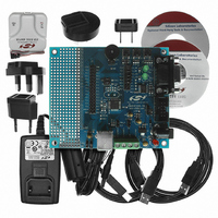
DEV KIT FOR C8051F320/F321
Manufacturer
Silicon Laboratories Inc
Type
MCUr
Specifications of C8051F320DK
Contents
Evaluation Board, Power Supply, USB Cables, Adapter and Documentation
Processor To Be Evaluated
C8051F320/F321
Interface Type
USB
Silicon Manufacturer
Silicon Labs
Core Architecture
8051
Silicon Core Number
C8051F320
Silicon Family Name
C8051F32x
Lead Free Status / RoHS Status
Contains lead / RoHS non-compliant
For Use With/related Products
Silicon Laboratories C8051F320, C8051F321
Lead Free Status / Rohs Status
Lead free / RoHS Compliant
Other names
336-1260
Available stocks
Company
Part Number
Manufacturer
Quantity
Price
Company:

Part Number:
C8051F320DK
Manufacturer:
SiliconL
Quantity:
4


C8051F320/1
4.
30
CNVSTR
REGIN
XTAL1
XTAL2
Pinout and Package Definitions
Name
VBUS
/RST/
C2CK
VREF
P3.0/
P0.2/
P0.3/
P0.6/
P0.7/
GND
VDD
P0.0
P0.1
P0.4
P0.5
P1.0
C2D
D+
D-
Pin Numbers
‘F320
10
32
31
30
29
28
27
26
6
3
9
7
8
4
5
2
1
Table 4.1. Pin Definitions for the C8051F320/1
‘F321
10
28
27
26
25
24
23
22
6
3
9
7
8
4
5
2
1
Power In
Power In 5 V Regulator Input. This pin is the input to the on-chip volt-
A I/O or
D I/O or
Power
D I/O
D I/O
D I/O
D I/O
D I/O
D I/O
D I/O
D I/O
D I/O
D I/O
D I/O
D I/O
D I/O
A I/O
Type
D In
D In
A In
A In
Out
Description
2.7-3.6 V Power Supply Voltage Input.
3.3 V Voltage Regulator Output. See Section 8.
Ground.
Device Reset. Open-drain output of internal POR or VDD
monitor. An external source can initiate a system reset by
driving this pin low for at least 15 µs. See Section 10.
Clock signal for the C2 Debug Interface.
Port 3.0. See Section 14 for a complete description.
Bi-directional data signal for the C2 Debug Interface.
age regulator.
VBUS Sense Input. This pin should be connected to the
VBUS signal of a USB network. A 5 V signal on this pin indi-
cates a USB network connection.
USB D+.
USB D–.
Port 0.0. See Section 14 for a complete description of Port 0.
Port 0.1.
Port 0.2.
External Clock Input. This pin is the external oscillator return
for a crystal or resonator. See Section 13.
Port 0.3.
External Clock Output. This pin is the excitation driver for an
external crystal or resonator, or an external clock input for
CMOS, capacitor, or RC oscillator configurations. See Sec-
tion 13.
Port 0.4.
Port 0.5.
Port 0.6.
ADC0 External Convert Start Input. See Section 5.
Port 0.7.
External VREF input or output. See Section 6.
Port 1.0. See Section 14 for a complete description of Port 1.
Rev. 1.4
Related parts for C8051F320DK
Image
Part Number
Description
Manufacturer
Datasheet
Request
R

Part Number:
Description:
SMD/C°/SINGLE-ENDED OUTPUT SILICON OSCILLATOR
Manufacturer:
Silicon Laboratories Inc
Part Number:
Description:
Manufacturer:
Silicon Laboratories Inc
Datasheet:
Part Number:
Description:
N/A N/A/SI4010 AES KEYFOB DEMO WITH LCD RX
Manufacturer:
Silicon Laboratories Inc
Datasheet:
Part Number:
Description:
N/A N/A/SI4010 SIMPLIFIED KEY FOB DEMO WITH LED RX
Manufacturer:
Silicon Laboratories Inc
Datasheet:
Part Number:
Description:
N/A/-40 TO 85 OC/EZLINK MODULE; F930/4432 HIGH BAND (REV E/B1)
Manufacturer:
Silicon Laboratories Inc
Part Number:
Description:
EZLink Module; F930/4432 Low Band (rev e/B1)
Manufacturer:
Silicon Laboratories Inc
Part Number:
Description:
I°/4460 10 DBM RADIO TEST CARD 434 MHZ
Manufacturer:
Silicon Laboratories Inc
Part Number:
Description:
I°/4461 14 DBM RADIO TEST CARD 868 MHZ
Manufacturer:
Silicon Laboratories Inc
Part Number:
Description:
I°/4463 20 DBM RFSWITCH RADIO TEST CARD 460 MHZ
Manufacturer:
Silicon Laboratories Inc
Part Number:
Description:
I°/4463 20 DBM RADIO TEST CARD 868 MHZ
Manufacturer:
Silicon Laboratories Inc
Part Number:
Description:
I°/4463 27 DBM RADIO TEST CARD 868 MHZ
Manufacturer:
Silicon Laboratories Inc
Part Number:
Description:
I°/4463 SKYWORKS 30 DBM RADIO TEST CARD 915 MHZ
Manufacturer:
Silicon Laboratories Inc
Part Number:
Description:
N/A N/A/-40 TO 85 OC/4463 RFMD 30 DBM RADIO TEST CARD 915 MHZ
Manufacturer:
Silicon Laboratories Inc
Part Number:
Description:
I°/4463 20 DBM RADIO TEST CARD 169 MHZ
Manufacturer:
Silicon Laboratories Inc