C8051F930DK Silicon Laboratories Inc, C8051F930DK Datasheet - Page 171
C8051F930DK
Manufacturer Part Number
C8051F930DK
Description
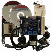
KIT DEV C8051F920,F921,F930,F931
Manufacturer
Silicon Laboratories Inc
Type
MCUr
Specifications of C8051F930DK
Contents
Target Board, Power Adapter, USB Debug Adapter, Cables, Batteries, and Software
Processor To Be Evaluated
C8051F930
Processor Series
C8051F9xx
Data Bus Width
8 bit
Interface Type
I2C, UART, SPI
Maximum Operating Temperature
+ 85 C
Minimum Operating Temperature
- 40 C
Operating Supply Voltage
0.9 V to 3.6 V
Lead Free Status / RoHS Status
Lead free / RoHS Compliant
For Use With/related Products
C8051F920, F921, F930, F931
Lead Free Status / Rohs Status
Lead free / RoHS Compliant
Other names
336-1473
Available stocks
Company
Part Number
Manufacturer
Quantity
Price
Company:

Part Number:
C8051F930DK
Manufacturer:
Silicon Labs
Quantity:
135


16. On-Chip DC-DC Converter (DC0)
C8051F93x-C8051F92x devices include an on-chip dc-dc converter to allow operation from a single cell
battery with a supply voltage as low as 0.9 V. The dc-dc converter is a switching boost converter with an
input voltage range of 0.9 to 1.8 V and a programmable output voltage range of 1.8 to 3.3 V. The default
output voltage is 1.9 V. The dc-dc converter can supply the system with up to 65 mW of regulated power
(or up to 100 mW in some applications) and can be used for powering other devices in the system. This
allows the most flexibility when interfacing to sensors and other analog signals which typically require a
higher supply voltage than a single-cell battery can provide.
Figure 16.1 shows a block diagram of the dc-dc converter. During normal operation in the first half of the
switching cycle, the Duty Cycle Control switch is closed and the Diode Bypass switch is open. Since the
output voltage is higher than the voltage at the DCEN pin, no current flows through the diode and the load
is powered from the output capacitor. During this stage, the DCEN pin is connected to ground through the
Duty Cycle Control switch, generating a positive voltage across the inductor and forcing its current to ramp
up.
In the second half of the switching cycle, the Duty Cycle control switch is opened and the Diode Bypass
switch is closed. This connects DCEN directly to VDD/DC+ and forces the inductor current to charge the
output capacitor. Once the inductor transfers its stored energy to the output capacitor, the Duty Cycle Con-
trol switch is closed, the Diode Bypass switch is opened, and the cycle repeats.
The dc-dc converter has a built in voltage reference and oscillator, and will automatically limit or turn off the
switching activity in case the peak inductor current rises beyond a safe limit or the output voltage rises
above the programmed target value. This allows the dc-dc converter output to be safely overdriven by a
secondary power source (when available) in order to preserve battery life. The dc-dc converter’s settings
can be modified using SFR registers which provide the ability to change the target output voltage, oscillator
frequency or source, Diode Bypass switch resistance, peak inductor current, and minimum duty cycle.
4.7 uF
0.68 uH
VBAT
DCEN
GND
Figure 16.1. DC-DC Converter Block Diagram
L
Control
Cycle
Duty
parasitic
DC0CN
DC0CF
Bypass
Diode
Rev. 1.1
Control Logic
C8051F93x-C8051F92x
DC/DC Converter
Reference
Oscillator
Voltage
DC/DC
L
parasitic
GND/DC-
1uF
VDD/DC+
I
load
C
load
171
Related parts for C8051F930DK
Image
Part Number
Description
Manufacturer
Datasheet
Request
R

Part Number:
Description:
SMD/C°/SINGLE-ENDED OUTPUT SILICON OSCILLATOR
Manufacturer:
Silicon Laboratories Inc
Part Number:
Description:
Manufacturer:
Silicon Laboratories Inc
Datasheet:
Part Number:
Description:
N/A N/A/SI4010 AES KEYFOB DEMO WITH LCD RX
Manufacturer:
Silicon Laboratories Inc
Datasheet:
Part Number:
Description:
N/A N/A/SI4010 SIMPLIFIED KEY FOB DEMO WITH LED RX
Manufacturer:
Silicon Laboratories Inc
Datasheet:
Part Number:
Description:
N/A/-40 TO 85 OC/EZLINK MODULE; F930/4432 HIGH BAND (REV E/B1)
Manufacturer:
Silicon Laboratories Inc
Part Number:
Description:
EZLink Module; F930/4432 Low Band (rev e/B1)
Manufacturer:
Silicon Laboratories Inc
Part Number:
Description:
I°/4460 10 DBM RADIO TEST CARD 434 MHZ
Manufacturer:
Silicon Laboratories Inc
Part Number:
Description:
I°/4461 14 DBM RADIO TEST CARD 868 MHZ
Manufacturer:
Silicon Laboratories Inc
Part Number:
Description:
I°/4463 20 DBM RFSWITCH RADIO TEST CARD 460 MHZ
Manufacturer:
Silicon Laboratories Inc
Part Number:
Description:
I°/4463 20 DBM RADIO TEST CARD 868 MHZ
Manufacturer:
Silicon Laboratories Inc
Part Number:
Description:
I°/4463 27 DBM RADIO TEST CARD 868 MHZ
Manufacturer:
Silicon Laboratories Inc
Part Number:
Description:
I°/4463 SKYWORKS 30 DBM RADIO TEST CARD 915 MHZ
Manufacturer:
Silicon Laboratories Inc
Part Number:
Description:
N/A N/A/-40 TO 85 OC/4463 RFMD 30 DBM RADIO TEST CARD 915 MHZ
Manufacturer:
Silicon Laboratories Inc
Part Number:
Description:
I°/4463 20 DBM RADIO TEST CARD 169 MHZ
Manufacturer:
Silicon Laboratories Inc