C8051F930DK Silicon Laboratories Inc, C8051F930DK Datasheet - Page 4
C8051F930DK
Manufacturer Part Number
C8051F930DK
Description
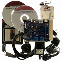
KIT DEV C8051F920,F921,F930,F931
Manufacturer
Silicon Laboratories Inc
Type
MCUr
Specifications of C8051F930DK
Contents
Target Board, Power Adapter, USB Debug Adapter, Cables, Batteries, and Software
Processor To Be Evaluated
C8051F930
Processor Series
C8051F9xx
Data Bus Width
8 bit
Interface Type
I2C, UART, SPI
Maximum Operating Temperature
+ 85 C
Minimum Operating Temperature
- 40 C
Operating Supply Voltage
0.9 V to 3.6 V
Lead Free Status / RoHS Status
Lead free / RoHS Compliant
For Use With/related Products
C8051F920, F921, F930, F931
Lead Free Status / Rohs Status
Lead free / RoHS Compliant
Other names
336-1473
Available stocks
Company
Part Number
Manufacturer
Quantity
Price
Company:

Part Number:
C8051F930DK
Manufacturer:
Silicon Labs
Quantity:
135


C8051F93x-C8051F92x
8. CIP-51 Microcontroller ......................................................................................... 100
9. Memory Organization........................................................................................... 109
10. External Data Memory Interface and On-Chip XRAM........................................ 113
11. Special Function Registers ................................................................................. 126
12. Interrupt Handler .................................................................................................. 133
13. Flash Memory ....................................................................................................... 145
4
7.2. Comparator Outputs ......................................................................................... 91
7.3. Comparator Response Time............................................................................. 92
7.4. Comparator Hysterisis ...................................................................................... 92
7.5. Comparator Register Descriptions.................................................................... 93
7.6. Comparator0 and Comparator1 Analog Multiplexers........................................ 97
8.1. Instruction Set ................................................................................................. 101
8.2. CIP-51 Register Descriptions.......................................................................... 106
9.1. Program Memory ............................................................................................ 110
9.2. Data Memory .................................................................................................. 111
10.1.Accessing XRAM............................................................................................ 113
10.2.Configuring the External Memory Interface for Off-Chip Access.................... 114
10.3.External Memory Interface Port Input/Output Configuration........................... 114
10.4.Multiplexed External Memory Interface .......................................................... 115
10.5.External Memory Interface Operating Modes................................................. 117
10.6.External Memory Interface Timing.................................................................. 118
10.7.EMIF Special Function Registers ................................................................... 119
10.8.EMIF Timing Diagrams................................................................................... 122
11.1.SFR Paging .................................................................................................... 127
12.1.Enabling Interrupt Sources ............................................................................. 133
12.2.MCU Interrupt Sources and Vectors............................................................... 133
12.3.Interrupt Priorities ........................................................................................... 134
12.4.Interrupt Latency............................................................................................. 134
12.5.Interrupt Register Descriptions ....................................................................... 136
12.6.External Interrupts INT0 and INT1.................................................................. 143
13.1.Programming The Flash Memory ................................................................... 145
8.1.1. Instruction and CPU Timing ................................................................... 101
9.1.1. MOVX Instruction and Program Memory ............................................... 110
9.2.1. Internal RAM .......................................................................................... 111
9.2.2. External RAM ......................................................................................... 112
10.1.1.16-Bit MOVX Example ........................................................................... 113
10.1.2.8-Bit MOVX Example ............................................................................. 113
10.5.1.Internal XRAM Only ............................................................................... 117
10.5.2.Split Mode without Bank Select.............................................................. 117
10.5.3.Split Mode with Bank Select................................................................... 118
10.5.4.External Only.......................................................................................... 118
10.8.1.Multiplexed 16-bit MOVX: EMI0CF[3:2] = 01, 10, or 11......................... 122
10.8.2.Multiplexed 8-bit MOVX without Bank Select: EMI0CF[3:2] = 01 or 11. 123
13.1.1.Flash Lock and Key Functions ............................................................... 145
13.1.2.Flash Erase Procedure .......................................................................... 146
Rev. 1.1
Related parts for C8051F930DK
Image
Part Number
Description
Manufacturer
Datasheet
Request
R

Part Number:
Description:
SMD/C°/SINGLE-ENDED OUTPUT SILICON OSCILLATOR
Manufacturer:
Silicon Laboratories Inc
Part Number:
Description:
Manufacturer:
Silicon Laboratories Inc
Datasheet:
Part Number:
Description:
N/A N/A/SI4010 AES KEYFOB DEMO WITH LCD RX
Manufacturer:
Silicon Laboratories Inc
Datasheet:
Part Number:
Description:
N/A N/A/SI4010 SIMPLIFIED KEY FOB DEMO WITH LED RX
Manufacturer:
Silicon Laboratories Inc
Datasheet:
Part Number:
Description:
N/A/-40 TO 85 OC/EZLINK MODULE; F930/4432 HIGH BAND (REV E/B1)
Manufacturer:
Silicon Laboratories Inc
Part Number:
Description:
EZLink Module; F930/4432 Low Band (rev e/B1)
Manufacturer:
Silicon Laboratories Inc
Part Number:
Description:
I°/4460 10 DBM RADIO TEST CARD 434 MHZ
Manufacturer:
Silicon Laboratories Inc
Part Number:
Description:
I°/4461 14 DBM RADIO TEST CARD 868 MHZ
Manufacturer:
Silicon Laboratories Inc
Part Number:
Description:
I°/4463 20 DBM RFSWITCH RADIO TEST CARD 460 MHZ
Manufacturer:
Silicon Laboratories Inc
Part Number:
Description:
I°/4463 20 DBM RADIO TEST CARD 868 MHZ
Manufacturer:
Silicon Laboratories Inc
Part Number:
Description:
I°/4463 27 DBM RADIO TEST CARD 868 MHZ
Manufacturer:
Silicon Laboratories Inc
Part Number:
Description:
I°/4463 SKYWORKS 30 DBM RADIO TEST CARD 915 MHZ
Manufacturer:
Silicon Laboratories Inc
Part Number:
Description:
N/A N/A/-40 TO 85 OC/4463 RFMD 30 DBM RADIO TEST CARD 915 MHZ
Manufacturer:
Silicon Laboratories Inc
Part Number:
Description:
I°/4463 20 DBM RADIO TEST CARD 169 MHZ
Manufacturer:
Silicon Laboratories Inc