C8051F930DK Silicon Laboratories Inc, C8051F930DK Datasheet - Page 23
C8051F930DK
Manufacturer Part Number
C8051F930DK
Description
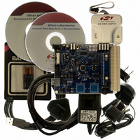
KIT DEV C8051F920,F921,F930,F931
Manufacturer
Silicon Laboratories Inc
Type
MCUr
Specifications of C8051F930DK
Contents
Target Board, Power Adapter, USB Debug Adapter, Cables, Batteries, and Software
Processor To Be Evaluated
C8051F930
Processor Series
C8051F9xx
Data Bus Width
8 bit
Interface Type
I2C, UART, SPI
Maximum Operating Temperature
+ 85 C
Minimum Operating Temperature
- 40 C
Operating Supply Voltage
0.9 V to 3.6 V
Lead Free Status / RoHS Status
Lead free / RoHS Compliant
For Use With/related Products
C8051F920, F921, F930, F931
Lead Free Status / Rohs Status
Lead free / RoHS Compliant
Other names
336-1473
Available stocks
Company
Part Number
Manufacturer
Quantity
Price
Company:

Part Number:
C8051F930DK
Manufacturer:
Silicon Labs
Quantity:
135


1.4.
An on-chip Programmable Counter/Timer Array (PCA) is included in addition to the four 16-bit general pur-
pose counter/timers. The PCA consists of a dedicated 16-bit counter/timer time base with six programma-
ble capture/compare modules. The PCA clock is derived from one of six sources: the system clock divided
by 12, the system clock divided by 4, Timer 0 overflows, an External Clock Input (ECI), the system clock, or
the external oscillator clock source divided by 8.
Each capture/compare module can be configured to operate in a variety of modes: edge-triggered capture,
software timer, high-speed output, pulse width modulator (8, 9, 10, 11, or 16-bit), or frequency output. Addi-
tionally, Capture/Compare Module 5 offers watchdog timer (WDT) capabilities. Following a system reset,
Module 5 is configured and enabled in WDT mode. The PCA Capture/Compare Module I/O and External
Clock Input may be routed to Port I/O via the Digital Crossbar.
1.5.
C8051F93x-C8051F92x devices have a 300 ksps, 10-bit successive-approximation-register (SAR) ADC
with integrated track-and-hold and programmable window detector. ADC0 also has an autonomous low
power Burst Mode which can automatically enable ADC0, capture and accumulate samples, then place
ADC0 in a low power shutdown mode without CPU intervention. It also has a 16-bit accumulator that can
automatically average the ADC results, providing an effective 11, 12, or 13 bit ADC result without any addi-
tional CPU intervention.
Programmable Counter Array
10-Bit SAR ADC with 16-bit Auto-Averaging Accumulator and Autonomous
Low Power Burst Mode
Capture/ Compare
Module 0
SYSCLK
SYSCLK 4
External Clock
ECI
SYSCLK
Timer Overflow
0
/12
/
/
8
Capture/ Compare
CLOCK
Module 1
MUX
PCA
Figure 1.6. PCA Block Diagram
16 -Bit Counter/Timer
Capture/ Compare
Port I/O
Module 2
Rev. 1.1
Crossbar
C8051F93x-C8051F92x
Capture/ Compare
Module 3
Capture/ Compare
Module 4
Capture/ Compare
Module 5 / WDT
23
Related parts for C8051F930DK
Image
Part Number
Description
Manufacturer
Datasheet
Request
R

Part Number:
Description:
SMD/C°/SINGLE-ENDED OUTPUT SILICON OSCILLATOR
Manufacturer:
Silicon Laboratories Inc
Part Number:
Description:
Manufacturer:
Silicon Laboratories Inc
Datasheet:
Part Number:
Description:
N/A N/A/SI4010 AES KEYFOB DEMO WITH LCD RX
Manufacturer:
Silicon Laboratories Inc
Datasheet:
Part Number:
Description:
N/A N/A/SI4010 SIMPLIFIED KEY FOB DEMO WITH LED RX
Manufacturer:
Silicon Laboratories Inc
Datasheet:
Part Number:
Description:
N/A/-40 TO 85 OC/EZLINK MODULE; F930/4432 HIGH BAND (REV E/B1)
Manufacturer:
Silicon Laboratories Inc
Part Number:
Description:
EZLink Module; F930/4432 Low Band (rev e/B1)
Manufacturer:
Silicon Laboratories Inc
Part Number:
Description:
I°/4460 10 DBM RADIO TEST CARD 434 MHZ
Manufacturer:
Silicon Laboratories Inc
Part Number:
Description:
I°/4461 14 DBM RADIO TEST CARD 868 MHZ
Manufacturer:
Silicon Laboratories Inc
Part Number:
Description:
I°/4463 20 DBM RFSWITCH RADIO TEST CARD 460 MHZ
Manufacturer:
Silicon Laboratories Inc
Part Number:
Description:
I°/4463 20 DBM RADIO TEST CARD 868 MHZ
Manufacturer:
Silicon Laboratories Inc
Part Number:
Description:
I°/4463 27 DBM RADIO TEST CARD 868 MHZ
Manufacturer:
Silicon Laboratories Inc
Part Number:
Description:
I°/4463 SKYWORKS 30 DBM RADIO TEST CARD 915 MHZ
Manufacturer:
Silicon Laboratories Inc
Part Number:
Description:
N/A N/A/-40 TO 85 OC/4463 RFMD 30 DBM RADIO TEST CARD 915 MHZ
Manufacturer:
Silicon Laboratories Inc
Part Number:
Description:
I°/4463 20 DBM RADIO TEST CARD 169 MHZ
Manufacturer:
Silicon Laboratories Inc