C8051T630DK Silicon Laboratories Inc, C8051T630DK Datasheet - Page 43
C8051T630DK
Manufacturer Part Number
C8051T630DK
Description
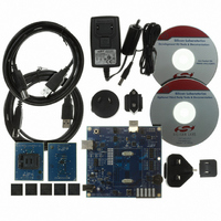
KIT DEV FOR C8051T630 FAMILY
Manufacturer
Silicon Laboratories Inc
Type
MCUr
Specifications of C8051T630DK
Contents
Board, daughter boards, power adapter, cables, documentation and software
Processor To Be Evaluated
C8051T63x
Interface Type
USB
Lead Free Status / RoHS Status
Lead free / RoHS Compliant
For Use With/related Products
C8051T630, T631, T632, T633, T634 and T635 MCUs
For Use With
336-1465 - BOARD SOCKET DAUGHTER 20-QFN
Lead Free Status / Rohs Status
Lead free / RoHS Compliant
Other names
336-1464


6.5. ADC0 Analog Multiplexer (C8051T630/2/4 only)
ADC0 on the C8051T630/2/4 uses an analog input multiplexer to select the positive input to the ADC. Any
of the following may be selected as the positive input: Port 0 and 1 I/O pins, the on-chip temperature sen-
sor, or the positive power supply (V
described in SFR Definition 6.9.
Important Note About ADC0 Input Configuration: Port pins selected as ADC0 inputs should be config-
ured as analog inputs, and should be skipped by the Digital Crossbar. To configure a Port pin for analog
input, set to 0 the corresponding bit in register PnMDIN. To force the Crossbar to skip a Port pin, set to 1
the corresponding bit in register PnSKIP. See Section “20. Port Input/Output” on page 109 for more Port
I/O configuration details.
Sensor
Temp
Figure 6.6. ADC0 Multiplexer Block Diagram
P0.0
P1.7
VDD
DD
). The ADC0 input channel is selected in the AMX0P register
AMX0P
Rev. 1.0
AMUX
C8051T630/1/2/3/4/5
ADC0
43
Related parts for C8051T630DK
Image
Part Number
Description
Manufacturer
Datasheet
Request
R

Part Number:
Description:
SMD/C°/SINGLE-ENDED OUTPUT SILICON OSCILLATOR
Manufacturer:
Silicon Laboratories Inc
Part Number:
Description:
Manufacturer:
Silicon Laboratories Inc
Datasheet:
Part Number:
Description:
N/A N/A/SI4010 AES KEYFOB DEMO WITH LCD RX
Manufacturer:
Silicon Laboratories Inc
Datasheet:
Part Number:
Description:
N/A N/A/SI4010 SIMPLIFIED KEY FOB DEMO WITH LED RX
Manufacturer:
Silicon Laboratories Inc
Datasheet:
Part Number:
Description:
N/A/-40 TO 85 OC/EZLINK MODULE; F930/4432 HIGH BAND (REV E/B1)
Manufacturer:
Silicon Laboratories Inc
Part Number:
Description:
EZLink Module; F930/4432 Low Band (rev e/B1)
Manufacturer:
Silicon Laboratories Inc
Part Number:
Description:
I°/4460 10 DBM RADIO TEST CARD 434 MHZ
Manufacturer:
Silicon Laboratories Inc
Part Number:
Description:
I°/4461 14 DBM RADIO TEST CARD 868 MHZ
Manufacturer:
Silicon Laboratories Inc
Part Number:
Description:
I°/4463 20 DBM RFSWITCH RADIO TEST CARD 460 MHZ
Manufacturer:
Silicon Laboratories Inc
Part Number:
Description:
I°/4463 20 DBM RADIO TEST CARD 868 MHZ
Manufacturer:
Silicon Laboratories Inc
Part Number:
Description:
I°/4463 27 DBM RADIO TEST CARD 868 MHZ
Manufacturer:
Silicon Laboratories Inc
Part Number:
Description:
I°/4463 SKYWORKS 30 DBM RADIO TEST CARD 915 MHZ
Manufacturer:
Silicon Laboratories Inc
Part Number:
Description:
N/A N/A/-40 TO 85 OC/4463 RFMD 30 DBM RADIO TEST CARD 915 MHZ
Manufacturer:
Silicon Laboratories Inc
Part Number:
Description:
I°/4463 20 DBM RADIO TEST CARD 169 MHZ
Manufacturer:
Silicon Laboratories Inc