MCB2470 Keil, MCB2470 Datasheet - Page 27
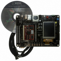
MCB2470
Manufacturer Part Number
MCB2470
Description
BOARD EVAL NXP LPC247X SERIES
Manufacturer
Keil
Type
MCUr
Specifications of MCB2470
Contents
Board, Cable, CD
For Use With/related Products
LPC2478
Lead Free Status / RoHS Status
Lead free / RoHS Compliant


NXP Semiconductors
LPC2478_1
Preliminary data sheet
7.2 On-chip flash programming memory
7.3 On-chip SRAM
7.4 Memory map
Pipeline techniques are employed so that all parts of the processing and memory systems
can operate continuously. Typically, while one instruction is being executed, its successor
is being decoded, and a third instruction is being fetched from memory.
The ARM7TDMI-S processor also employs a unique architectural strategy known as
Thumb, which makes it ideally suited to high-volume applications with memory
restrictions, or applications where code density is an issue.
The key idea behind Thumb is that of a super-reduced instruction set. Essentially, the
ARM7TDMI-S processor has two instruction sets:
The Thumb set’s 16-bit instruction length allows it to approach higher density compared to
standard ARM code while retaining most of the ARM’s performance.
The LPC2478 incorporates 512 kB flash memory system. This memory may be used for
both code and data storage. Programming of the flash memory may be accomplished in
several ways. It may be programmed In System via the serial port (UART0). The
application program may also erase and/or program the flash while the application is
running, allowing a great degree of flexibility for data storage field and firmware upgrades.
The flash memory is 128 bits wide and includes pre-fetching and buffering techniques to
allow it to operate at speeds of 72 MHz.
The LPC2478 provides a minimum of 100000 write/erase cycles and 20 years of data
retention.
The LPC2478 includes a SRAM memory of 64 kB reserved for the ARM processor
exclusive use. This RAM may be used for code and/or data storage and may be accessed
as 8 bits, 16 bits, and 32 bits.
A 16 kB SRAM block serving as a buffer for the Ethernet controller and a 16 kB SRAM
associated with the second AHB bus can be used both for data and code storage, too.
Remaining SRAM such as a 4 kB USB FIFO and a 2 kB RTC SRAM can be used for data
storage only. The RTC SRAM is battery powered and retains the content in the absence of
the main power supply.
The LPC2478 memory map incorporates several distinct regions as shown in
Figure
In addition, the CPU interrupt vectors may be remapped to allow them to reside in either
flash memory (default), boot ROM, or SRAM (see
•
•
the standard 32-bit ARM set
a 16-bit Thumb set
4.
Rev. 01 — 9 February 2007
Section
7.27.6).
Fast communication chip
LPC2478
© NXP B.V. 2007. All rights reserved.
Table 5
27 of 76
and
Related parts for MCB2470
Image
Part Number
Description
Manufacturer
Datasheet
Request
R

Part Number:
Description:
KIT REF SYSTEM 78K0 UPD78F0712
Manufacturer:
Renesas Electronics America
Datasheet:
Part Number:
Description:
KIT DEMO EVAL 78K0R IE3
Manufacturer:
Renesas Electronics America
Datasheet:
Part Number:
Description:
KIT EVAL SYSTEM 78K0 UPD78F0714
Manufacturer:
Renesas Electronics America
Datasheet:

Part Number:
Description:
KEIL C-COMPILER INTERNATIONAL
Manufacturer:
Silicon Laboratories Inc
Part Number:
Description:
KEIL C-COMPILER US VERSION
Manufacturer:
Silicon Laboratories Inc

Part Number:
Description:
DEV KIT FOR STM32
Manufacturer:
STMicroelectronics
Datasheet:

Part Number:
Description:
KIT STARTER FOR STM32
Manufacturer:
STMicroelectronics
Datasheet:

Part Number:
Description:
KIT STARTER FOR STM32F10XE MCU
Manufacturer:
STMicroelectronics
Datasheet:

Part Number:
Description:
KIT STARTER KEIL FOR STR910
Manufacturer:
STMicroelectronics
Datasheet:


Part Number:
Description:
Microcontroller Modules & Accessories KEIL ULINK PRO 5V ADAPTOR KIT
Manufacturer:
Keil Software

Part Number:
Description:
BOARD EVAL FOR LPC213X ARM MCU
Manufacturer:
NXP Semiconductors
Datasheet:

Part Number:
Description:
K60N512 Keil Tower Kit
Manufacturer:
Freescale Semiconductor
Datasheet: