MCB2470 Keil, MCB2470 Datasheet - Page 47
MCB2470
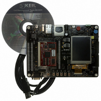
Manufacturer Part Number
MCB2470
Description
BOARD EVAL NXP LPC247X SERIES
Manufacturer
Keil
Type
MCUr
Specifications of MCB2470
Contents
Board, Cable, CD
For Use With/related Products
LPC2478
Lead Free Status / RoHS Status
Lead free / RoHS Compliant


NXP Semiconductors
LPC2478_1
Preliminary data sheet
7.27.3 Code security (Code Read Protection - CRP)
7.27.4 AHB bus
7.27.5 External interrupt inputs
The second stage of low-voltage detection asserts Reset to inactivate the LPC2478 when
the voltage on the V
flash as operation of the various elements of the chip would otherwise become unreliable
due to low voltage. The BOD circuit maintains this reset down below 1 V, at which point
the power-on reset circuitry maintains the overall Reset.
Both the 2.95 V and 2.65 V thresholds include some hysteresis. In normal operation, this
hysteresis allows the 2.95 V detection to reliably interrupt, or a regularly-executed event
loop to sense the condition.
This feature of the LPC2478 allows user to enable different levels of security in the system
so that access to the on-chip flash and use of the JTAG and ISP can be restricted. When
needed, CRP is invoked by programming a specific pattern into a dedicated flash location.
IAP commands are not affected by the CRP.
There are three levels of the Code Read Protection.
CRP1 disables access to chip via the JTAG and allows partial flash update (excluding
flash sector 0) using a limited set of the ISP commands. This mode is useful when CRP is
required and flash field updates are needed but all sectors can not be erased.
CRP2 disables access to chip via the JTAG and only allows full flash erase and update
using a reduced set of the ISP commands.
Running an application with level CRP3 selected fully disables any access to chip via the
JTAG pins and the ISP. This mode effectively disables ISP override using P2[10] pin, too.
It is up to the user’s application to provide (if needed) flash update mechanism using IAP
calls or a call to reinvoke the ISP command to enable flash update via UART0.
Remark: when CRP3 level of protection is invoked, no future factory testing can be
performed on the device.
The LPC2478 implements two AHB buses in order to allow the Ethernet block to operate
without interference caused by other system activity. The primary AHB, referred to as
AHB1, includes the Vectored Interrupt Controller, GPDMA controller, USB interface, and
16 kB SRAM.
The second AHB, referred to as AHB2, includes only the Ethernet block and an
associated 16 kB SRAM. In addition, a bus bridge is provided that allows the secondary
AHB to be a bus master on AHB1, allowing expansion of Ethernet buffer space into
off-chip memory or unused space in memory residing on AHB1.
In summary, bus masters with access to AHB1 are the ARM7 itself, the USB block, the
GPDMA function, and the Ethernet block (via the bus bridge from AHB2). Bus masters
with access to AHB2 are the ARM7 and the Ethernet block.
The LPC2478 includes up to 68 edge sensitive interrupt inputs combined with up to four
level sensitive external interrupt inputs as selectable pin functions. The external interrupt
inputs can optionally be used to wake up the processor from Power-down mode.
DD(3V3)
Rev. 01 — 9 February 2007
pins falls below 2.65 V. This Reset prevents alteration of the
Fast communication chip
LPC2478
© NXP B.V. 2007. All rights reserved.
47 of 76
Related parts for MCB2470
Image
Part Number
Description
Manufacturer
Datasheet
Request
R

Part Number:
Description:
KIT REF SYSTEM 78K0 UPD78F0712
Manufacturer:
Renesas Electronics America
Datasheet:
Part Number:
Description:
KIT DEMO EVAL 78K0R IE3
Manufacturer:
Renesas Electronics America
Datasheet:
Part Number:
Description:
KIT EVAL SYSTEM 78K0 UPD78F0714
Manufacturer:
Renesas Electronics America
Datasheet:

Part Number:
Description:
KEIL C-COMPILER INTERNATIONAL
Manufacturer:
Silicon Laboratories Inc
Part Number:
Description:
KEIL C-COMPILER US VERSION
Manufacturer:
Silicon Laboratories Inc

Part Number:
Description:
DEV KIT FOR STM32
Manufacturer:
STMicroelectronics
Datasheet:

Part Number:
Description:
KIT STARTER FOR STM32
Manufacturer:
STMicroelectronics
Datasheet:

Part Number:
Description:
KIT STARTER FOR STM32F10XE MCU
Manufacturer:
STMicroelectronics
Datasheet:

Part Number:
Description:
KIT STARTER KEIL FOR STR910
Manufacturer:
STMicroelectronics
Datasheet:


Part Number:
Description:
Microcontroller Modules & Accessories KEIL ULINK PRO 5V ADAPTOR KIT
Manufacturer:
Keil Software

Part Number:
Description:
BOARD EVAL FOR LPC213X ARM MCU
Manufacturer:
NXP Semiconductors
Datasheet:

Part Number:
Description:
K60N512 Keil Tower Kit
Manufacturer:
Freescale Semiconductor
Datasheet: