DK-EMB-3C120N Altera, DK-EMB-3C120N Datasheet
DK-EMB-3C120N
Specifications of DK-EMB-3C120N
Available stocks


Related parts for DK-EMB-3C120N


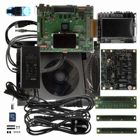
DK-EMB-3C120N Summary of contents
Page 1
... Cyclone III FPGA Development Kit User Guide 101 Innovation Drive San Jose, CA 95134 www.altera.com UG-01027-1.4 P25-36208-03 Cyclone III FPGA Development Kit User Guide Subscribe ...
Page 2
... Altera warrants performance of its semiconductor products to current specifications in accordance with Altera’s standard warranty, but reserves the right to make changes to any products and services at any time without notice. Altera assumes no responsibility or liability arising out of the application or use of any information, product, or service described herein except as expressly agreed to in writing by Altera. Altera customers are advised to obtain the latest version of device specifications before relying on any published information and before placing orders for products or services ...
Page 3
... MAX II Registers . . . . . . . . . . . . . . . . . . . . . . . . . . . . . . . . . . . . . . . . . . . . . . . . . . . . . . . . . . . . . . . . . . . 6–4 JTAG Chain . . . . . . . . . . . . . . . . . . . . . . . . . . . . . . . . . . . . . . . . . . . . . . . . . . . . . . . . . . . . . . . . . . . . . . . . 6–4 Board Information . . . . . . . . . . . . . . . . . . . . . . . . . . . . . . . . . . . . . . . . . . . . . . . . . . . . . . . . . . . . . . . . . . 6–5 Flash Memory Map . . . . . . . . . . . . . . . . . . . . . . . . . . . . . . . . . . . . . . . . . . . . . . . . . . . . . . . . . . . . . . . . . 6–5 The GPIO Tab . . . . . . . . . . . . . . . . . . . . . . . . . . . . . . . . . . . . . . . . . . . . . . . . . . . . . . . . . . . . . . . . . . . . . . . . 6–5 Character LCD . . . . . . . . . . . . . . . . . . . . . . . . . . . . . . . . . . . . . . . . . . . . . . . . . . . . . . . . . . . . . . . . . . . . . 6–6 User DIP Switches . . . . . . . . . . . . . . . . . . . . . . . . . . . . . . . . . . . . . . . . . . . . . . . . . . . . . . . . . . . . . . . . . . 6–6 User LEDs . . . . . . . . . . . . . . . . . . . . . . . . . . . . . . . . . . . . . . . . . . . . . . . . . . . . . . . . . . . . . . . . . . . . . . . . . 6–6 Push Button Switches . . . . . . . . . . . . . . . . . . . . . . . . . . . . . . . . . . . . . . . . . . . . . . . . . . . . . . . . . . . . . . . 6–6 September 2010 Altera Corporation Contents Cyclone III FPGA Development Kit User Guide ...
Page 4
... Programming the Flash Device . . . . . . . . . . . . . . . . . . . . . . . . . . . . . . . . . . . . . . . . . . . . . . . . . . . . . . . . . . . A–4 Restoring the Factory Design to the Flash Device . . . . . . . . . . . . . . . . . . . . . . . . . . . . . . . . . . . . . . . . . . . A–6 Additional Information Document Revision History . . . . . . . . . . . . . . . . . . . . . . . . . . . . . . . . . . . . . . . . . . . . . . . . . . . . . . . . . . . Info–1 How to Contact Altera . . . . . . . . . . . . . . . . . . . . . . . . . . . . . . . . . . . . . . . . . . . . . . . . . . . . . . . . . . . . . . . . Info–1 Typographic Conventions . . . . . . . . . . . . . . . . . . . . . . . . . . . . . . . . . . . . . . . . . . . . . . . . . . . . . . . . . . . . . Info–2 Cyclone III FPGA Development Kit User Guide Contents September 2010 Altera Corporation ...
Page 5
... Verilog code to help you get started quickly with your own designs. The development board includes an Altera Cyclone III FPGA configured with a hardware reference design stored in flash memory. Hardware designers can use the development board, along with example designs included in the kit platform to prototype complex embedded systems ...
Page 6
... Program a device and verify your design in hardware ■ Nios II Embedded Software Design Tools—This full-featured set of tools allows ■ you to develop embedded software on the Nios II processor running on Altera FPGAs. ■ Cyclone III Development Kit Application and Drivers—The application and drivers allow you to execute memory read and write transactions to the board. ...
Page 7
... This user guide familiarizes you with the contents of the kit and guides you through the Cyclone III development board setup. Using this guide, you can do the following: Inspect the contents of the kit ■ Install the Altera Quartus II Web Edition software ■ ■ Install the Cyclone III Development Kit ■ ...
Page 8
... DLL for the .NET application. You can download the .NET framework application from the following location: www.microsoft.com/download. Cyclone III FPGA Development Kit User Guide Chapter 2: Getting Started FPGAs. Quartus II Web Edition for further information on the “Licensing Considerations” on page September 2010 Altera Corporation Before You Begin 3–3. ...
Page 9
... Additional daughter cards available for purchase Cyclone III handbook Cyclone III reference designs eStore if you want to purchase devices Cyclone III Orcad symbols ® Nios II 32-bit embedded processor solutions September 2010 Altera Corporation Refer to www.altera.com/products/devkits/kit-daughter_boards.jsp www.altera.com/literature/lit-cyc3.jsp http://www.altera.com/products/devkits/altera/kit-cyc3.html www.altera.com/buy/devices/buy-devices.html www.altera.com/support/software/download/pcb/pcbpcb_index.html www.altera.com/technology/embedded/emb-index.html Cyclone III FPGA Development Kit User Guide ...
Page 10
... Cyclone III FPGA Development Kit User Guide Chapter 2: Getting Started References September 2010 Altera Corporation ...
Page 11
... Cyclone III Development Kit installation directory. Figure 3–1. Cyclone III Development Kit Installed Directory Structure September 2010 Altera Corporation 3. Software Installation page of the Altera website. Alternatively, you can request a Development Kits, Daughter Cards & page of the Altera website. <path> The default Windows installation directory is C:\altera\ <version#> \kits. ...
Page 12
... Installing the Quartus II Web Edition Software The Quartus II Web Edition software provides the necessary tools for developing hardware and software for Altera FPGAs. Included in the Quartus II Web Edition software are the Quartus II software, the Nios II EDS, and the MegaCore The Quartus II software (including SOPC Builder) and the Nios II EDS are the primary FPGA development tools for creating the reference designs in this kit ...
Page 13
... The Cyclone III development board includes integrated USB-Blaster™ circuitry for FPGA programming. However, for the host computer and development board to communicate, you must install the USB-Blaster driver on the host computer download the USB-Blaster driver the Altera support site at www.altera.com/support/software/drivers/dri-index.html. To install it blaster-xp.html. ...
Page 14
... Cyclone III FPGA Development Kit User Guide Chapter 3: Software Installation Installing the USB-Blaster Driver September 2010 Altera Corporation ...
Page 15
... FPGA programming. Host computer and development board cannot communicate without the USB-Blaster driver software installed. For installation information, refer to “Installing the USB-Blaster Driver” on page September 2010 Altera Corporation 4. Development Board Setup and have completed the 3–3. Cyclone III FPGA Development Kit User Guide ...
Page 16
... Clock Out SMA (J11) HSMC Port B Present LED (D19) PGM Config Select Rotary Switch (SW5) Board-Specific LEDs (D20 through D24) User Defined Reset and 7-Segment Factory Display (U30) Configuration Push Buttons (S6 and S7) Table 4–1. Default Position Position September 2010 Altera Corporation ...
Page 17
... Confirm that user LEDs 0-7 flash in a scrolling, side-to-side pattern. For customized configurations, the pattern depends on the application. f For information about custom configurations, refer to Flash Device” on page September 2010 Altera Corporation Function Name Position 0 RSV0 MAX_RESERVE0 RSV1 ...
Page 18
... Confirm that user LEDs 0-3 flash in a slow binary counting pattern. Cyclone III FPGA Development Kit User Guide 3–3. Table 4–2. Chapter 4: Development Board Setup Configuring the FPGA “Installing the USB-Blaster September 2010 Altera Corporation ...
Page 19
... FPGA designs to the FPGA design 1 and design 6 (HW1 and SW1) portion of flash memory, and provides links to useful information on the Altera website, including links to kit-specific and design resources. 1 After successfully updating the FPGA design 1 and design 6 (HW1 and SW1)flash memory, you can load the user design from flash memory into the FPGA ...
Page 20
... Board Update Portal web page the Hardware File Name field specify the .flash file that you either downloaded from the Altera website or created on your own. If there is a software component to the design, specify it in the same manner using the Software File Name field, otherwise leave the Software File Name field blank ...
Page 21
... The application allows you to exercise most of the board components. While using the application, you reconfigure the FPGA several times with test designs specific to the functionality you are testing. September 2010 Altera Corporation 6. Board Test System 3–1. Cyclone III FPGA Development Kit User Guide ...
Page 22
... Verify the settings for the board settings DIP switch bank (SW3) match the settings in Table 4–2 on page Cyclone III FPGA Development Kit User Guide Figure 6–1 shows the initial GUI for a board that is 4–3. Chapter 6: Board Test System Preparing the Board September 2010 Altera Corporation ...
Page 23
... BoardTestSystem.exe application Windows, click Start > All Programs > Altera > Cyclone III FPGA Development Kit <version> > Board Test System to run the application. A GUI appears, displaying the application tab that corresponds to the design running in the FPGA. The Cyclone III FPGA development board’s flash memory ships preconfigured with the design that corresponds to the Config, GPIO, SRAM& ...
Page 24
... The JTAG chain control shows all the devices currently in the JTAG chain. The Cyclone III device is always the first device in the chain. Cyclone III FPGA Development Kit User Guide shows the Config tab. The tab displays the contents of the Chapter 6: Board Test System Using the Board Test System September 2010 Altera Corporation ...
Page 25
... LEDs on or off, detect push button presses, write to the 7-segment display, and run an Ethernet application (the Simple Socket Server Test) on your board. shows the GPIO tab. Figure 6–3. The GPIO Tab September 2010 Altera Corporation 6–5 Figure 6–3 Cyclone III FPGA Development Kit User Guide ...
Page 26
... Click Start Simple Socket Server to load the application which allows you to interactively enter keyboard characters to select menu items. The application responds to the keypress and takes appropriate action. Cyclone III FPGA Development Kit User Guide Chapter 6: Board Test System Using the Board Test System September 2010 Altera Corporation ...
Page 27
... SRAM is 0x0000.0000 through 0x001F.FFFF, as shown in the GUI you enter an address outside of the 0x00000000 to 0x001FFF80 SRAM address space, a warning message identifies the valid SRAM address range. September 2010 Altera Corporation shows the SRAM&Flash tab. 6–7 Cyclone III FPGA Development Kit User Guide ...
Page 28
... Figure 6–1 on page Cyclone III FPGA Development Kit User Guide 6–2). September 2010 Altera Corporation Chapter 6: Board Test System Using the Board Test System ...
Page 29
... Load—displays the selected .bmp file on the graphic LCD. ■ 1 The graphic LCD supports only 128x64 size .bmp files. There are three sample .bmp files located in <install dir>\kits\cycloneIII_3c120_dev\examples\board_test_system directory. September 2010 Altera Corporation 6–9 Figure 6–3 Cyclone III FPGA Development Kit User Guide ...
Page 30
... The Start control initiates DDR2 memory transaction performance analysis. Stop The Stop control terminates transaction performance analysis. Cyclone III FPGA Development Kit User Guide Figure 6–6 shows the DDR2 tab when the board is configured Chapter 6: Board Test System Using the Board Test System September 2010 Altera Corporation ...
Page 31
... Write then read—selects read and write transactions for analysis. ■ ■ Read only—selects read transactions for analysis. ■ Write only—selects write transactions for analysis. September 2010 Altera Corporation 6–11 Cyclone III FPGA Development Kit User Guide ...
Page 32
... Cyclone III FPGA Development Kit User Guide Chapter 6: Board Test System Using the Board Test System September 2010 Altera Corporation ...
Page 33
... Button User_PB0 AD7 User_PB1 AC12 User_PB2 AH3 User_PB3 AA12 September 2010 Altera Corporation Table 7–3 on page 7–2, respectively, represent the percent of the full Type Reset Resets the demo to the beginning, i_nrst Advances the design example to the next higher frequency, Toggle i_nfreq_next ...
Page 34
... Similarly, the overall design 7–2) sets the toggle frequency of these I/O pins. Chapter 7: Power Measurement Power Design Example Frequency (MHz 100 LED2 Resources Number of (AF18) (%) Outputs 104 1 70 112 0 75 120 1 80 128 0 85 136 1 90 144 0 95 152 September 2010 Altera Corporation ...
Page 35
... This example uses FPGA I/O banks and 6. Using the SW4 settings measure the power for I/O banks 1 and 2, then for I/O banks 5 and 6, by performing the following steps: 1. Ensure that the 8-position SW1 DIP switch is configured to the default settings shown in September 2010 Altera Corporation FPGA Power 0 Core 1.2 V ...
Page 36
... Banks 1 and 2 2.5 V Banks 5 and 6 2.5 V 1.2 V CC_INT Chapter 7: Power Measurement Measuring Power “Configuring 7–1), advance through the 7–2. Notice how power increases Manual. Sense Resistor Resistor Value 0.009 Ω R48 0.009 Ω R51 0.009 Ω R49 September 2010 Altera Corporation ...
Page 37
... To change the number of outputs, modify the design example and assign the pins appropriately. 1 Power should track linearly with frequency and percentage resources. If you observe superlinear power measurements, some temperature issue may be the cause. September 2010 Altera Corporation Table 7–5. V SUPPLY × ...
Page 38
... Cyclone III FPGA Development Kit User Guide Chapter 7: Power Measurement Changing the Design Example September 2010 Altera Corporation ...
Page 39
... September 2010 Altera Corporation 8. Design Tutorials My First FPGA Design Tutorial provide step-by-step guidance for the first-time describes how to create a simple Altera FPGA design. My First FPGA Design Tutorial introduces the basic system development flow for the My First Nios II Software Tutorial Cyclone III FPGA Development Kit User Guide ...
Page 40
... Cyclone III FPGA Development Kit User Guide Chapter 8: Design Tutorials My First Nios II Software Tutorial September 2010 Altera Corporation ...
Page 41
... LEDs on the board flash sequentially from side to side. As you develop your own project using the Altera tools, you may wish to program the flash device so that, upon power up, it loads the FPGA with your own design. Or you may wish to restore the default factory configuration to your board ...
Page 42
... Browse to and select the file you wish to convert and click OK. Figure A–1 factory image your_design_name.sof. Cyclone III FPGA Development Kit User Guide Parallel Flash Loader Megafunction User shows the Convert Programming Files dialog box updated with the Appendix A: Programming the Flash Device Creating a Flash File Guide. September 2010 Altera Corporation ...
Page 43
... Click Generate. Generation takes a short time and it is confirmed by a “Generated… pof successfully” message. You now have a successfully generated .pof that can be programmed to the flash device to automatically configure the FPGA on your Cyclone III development board. September 2010 Altera Corporation A–3 Cyclone III FPGA Development Kit User Guide ...
Page 44
... Cyclone III FPGA Development Kit User Guide “Programming the Flash Guide. “Creating a Flash File” on page Appendix A: Programming the Flash Device Parallel Flash Loader Instantiation Device”, steps 1 through Parallel Flash Loader A–1. The following Table 4–2 on page 4–3. September 2010 Altera Corporation ...
Page 45
... Double-click the <File><none> field of the CFI_512MB row. The Select New Programming File dialog box appears. Select the desired .pof, in this example the <output_file>.pof flash file you created earlier, and click Open. September 2010 Altera Corporation A–5 (Figure A–2). ...
Page 46
... A–4, except select the cycloneIII_3c120_dev_factory_recovery.pof file. Cyclone III FPGA Development Kit User Guide Appendix A: Programming the Flash Device Restoring the Factory Design to the Flash Device (Figure A–3). This results in writes only 4–2. “Programming the Flash Device” on September 2010 Altera Corporation ...
Page 47
... Contact Technical support Technical training Product literature Non-technical support (General) (Software Licensing) Note to Table: (1) You can also contact your local Altera sales office or sales representative. September 2010 Altera Corporation Changes Chapter 5, Board Update Portal and Chapter 6, Board Test Figure 3–1 on page 3– ...
Page 48
... A warning calls attention to a condition or possible situation that can cause you injury. The envelope links to the Email Subscription Management Center website, where you can sign up to receive update notifications for Altera documents. Additional Information Typographic Conventions page of the Altera September 2010 Altera Corporation ...