DK-EMB-3C120N Altera, DK-EMB-3C120N Datasheet - Page 28
DK-EMB-3C120N
Manufacturer Part Number
DK-EMB-3C120N
Description
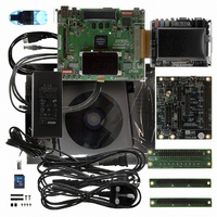
KIT DEV EMB CYCLONE III EDITION
Manufacturer
Altera
Series
Cyclone® IIIr
Type
FPGAr
Datasheets
1.DK-START-3C25N.pdf
(74 pages)
2.DK-DEV-3C120N.pdf
(48 pages)
3.DK-EMB-3C120N.pdf
(5 pages)
Specifications of DK-EMB-3C120N
Contents
Board, Cables, CD(s), USB-Blaster™, Power Supply
Architecture
PLD/FPGA
Silicon Manufacturer
Altera
Core Architecture
FPGA
Core Sub-architecture
Cyclone
Silicon Core Number
EP3C
Silicon Family Name
Cyclone III
Rohs Compliant
Yes
For Use With/related Products
EP3C120
Lead Free Status / RoHS Status
Lead free / RoHS Compliant
Other names
544-2589
Available stocks
Company
Part Number
Manufacturer
Quantity
Price
Company:

Part Number:
DK-EMB-3C120N
Manufacturer:
Altera
Quantity:
135


6–8
Cyclone III FPGA Development Kit User Guide
1
1
To update the SRAM contents, change values in the table and click Write. The
application writes the new values to SRAM and then reads the values back to
guarantee that the graphical display accurately reflects the memory contents.
Flash
The Flash control allows you to read and write the flash memory on your board. Type
a starting address in the text box and click Read. Values starting at the specified
address appear in the top row of the table. The flash memory addresses display in the
format the Nios II processor within the FPGA uses, that is, each flash memory address
is offset by 0x00000000. Thus, the first location in flash memory appears as 0x00000000
in the GUI. The base address of flash memory in this Nios II-based BTS design is
0x0800.0000. The valid address range within the 64-MB flash memory is 0x0000.0000
through 0x03FF.FFFF, as shown in the GUI.
If you enter an address outside of the 0x00000000 to 0x03FFFF80 flash memory
address space, a warning message identifies the valid flash memory address range.
To update the flash memory contents, change values in the table and click Write. The
application writes the new values to flash memory and then reads the values back to
guarantee that the graphical display accurately reflects the memory contents.
To prevent overwriting the dedicated portions of flash memory, the application limits
the writable flash memory address range from 0x07000000 to 0x0701FF80 (which
corresponds to the unused flash memory address range of 0x02000000 - 0x0201FF80
shown in
Figure 6–1 on page
6–2).
September 2010 Altera Corporation
Chapter 6: Board Test System
Using the Board Test System
Related parts for DK-EMB-3C120N
Image
Part Number
Description
Manufacturer
Datasheet
Request
R

Part Number:
Description:
CYCLONE II STARTER KIT EP2C20N
Manufacturer:
Altera
Datasheet:


Part Number:
Description:
CPLD, EP610 Family, ECMOS Process, 300 Gates, 16 Macro Cells, 16 Reg., 16 User I/Os, 5V Supply, 35 Speed Grade, 24DIP
Manufacturer:
Altera Corporation
Datasheet:
Part Number:
Description:
CPLD, EP610 Family, ECMOS Process, 300 Gates, 16 Macro Cells, 16 Reg., 16 User I/Os, 5V Supply, 15 Speed Grade, 24DIP
Manufacturer:
Altera Corporation
Datasheet:
Part Number:
Description:
Manufacturer:
Altera Corporation
Datasheet:
Part Number:
Description:
CPLD, EP610 Family, ECMOS Process, 300 Gates, 16 Macro Cells, 16 Reg., 16 User I/Os, 5V Supply, 30 Speed Grade, 24DIP
Manufacturer:
Altera Corporation
Datasheet:
Part Number:
Description:
High-performance, low-power erasable programmable logic devices with 8 macrocells, 10ns
Manufacturer:
Altera Corporation
Datasheet:
Part Number:
Description:
High-performance, low-power erasable programmable logic devices with 8 macrocells, 7ns
Manufacturer:
Altera Corporation
Datasheet:
Part Number:
Description:
Classic EPLD
Manufacturer:
Altera Corporation
Datasheet:
Part Number:
Description:
High-performance, low-power erasable programmable logic devices with 8 macrocells, 10ns
Manufacturer:
Altera Corporation
Datasheet:
Part Number:
Description:
Manufacturer:
Altera Corporation
Datasheet:
Part Number:
Description:
Manufacturer:
Altera Corporation
Datasheet:
Part Number:
Description:
Manufacturer:
Altera Corporation
Datasheet:
Part Number:
Description:
CPLD, EP610 Family, ECMOS Process, 300 Gates, 16 Macro Cells, 16 Reg., 16 User I/Os, 5V Supply, 25 Speed Grade, 24DIP
Manufacturer:
Altera Corporation
Datasheet: