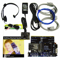
ADSP-3PARCBF548E02 Analog Devices Inc, ADSP-3PARCBF548E02 Datasheet - Page 11

ADSP-3PARCBF548E02
Manufacturer Part Number
ADSP-3PARCBF548E02
Description
KIT DEV STARTER BF548
Manufacturer
Analog Devices Inc
Series
Blackfin®r
Type
DSPr
Specifications of ADSP-3PARCBF548E02
Contents
Board, Cables, CD, Headset with Microphone, Module, Power Supply
For Use With/related Products
ADSP-BF548
Lead Free Status / RoHS Status
Lead free / RoHS Compliant
The ADSP-BF54x Blackfin processors’ DMA controllers sup-
port both 1-dimensional (1D) and 2-dimensional (2D) DMA
transfers. DMA transfer initialization can be implemented from
registers or from sets of parameters called descriptor blocks.
The 2D DMA capability supports arbitrary row and column
sizes up to 64K elements by 64K elements, and arbitrary row
and column step sizes up to ±32K elements. Furthermore, the
column step size can be less than the row step size, allowing
implementation of interleaved data streams. This feature is
especially useful in video applications where data can be de-
interleaved on the fly.
Examples of DMA types supported by the ADSP-BF54x
Blackfin processors’ DMA controllers include:
In addition to the dedicated peripheral DMA channels, the
DMAC1 and DMAC0 controllers each feature two memory
DMA channel pairs for transfers between the various memories
of the ADSP-BF54x Blackfin processors. This enables transfers
of blocks of data between any of the memories—including
external DDR, ROM, SRAM, and flash memory—with minimal
processor intervention. Like peripheral DMAs, memory DMA
transfers can be controlled by a very flexible descriptor-based
methodology or by a standard register-based autobuffer
mechanism.
The memory DMA channels of the DMAC1 controller
(MDMA2 and MDMA3) can be controlled optionally by the
external DMA request input pins. When used in conjunction
with the External Bus Interface Unit (EBIU), this handshaked
memory DMA (HMDMA) scheme can be used to efficiently
exchange data with block-buffered or FIFO-style devices con-
nected externally. Users can select whether the DMA request
pins control the source or the destination side of the memory
DMA. It allows control of the number of data transfers for
memory DMA. The number of transfers per edge is program-
mable. This feature can be programmed to allow memory DMA
to have an increased priority on the external bus relative to the
core.
Host DMA Port Interface
The host DMA port (HOSTDP) facilitates a host device external
to the ADSP-BF54x Blackfin processors to be a DMA master
and transfer data back and forth. The host device always masters
the transactions, and the processor is always a DMA slave
device.
The HOSTDP is enabled through the peripheral access bus.
Once the port has been enabled, the transactions are controlled
by the external host. The external host programs standard DMA
• A single, linear buffer that stops upon completion
• A circular, auto-refreshing buffer that interrupts on each
• 1D or 2D DMA using a linked list of descriptors
• 2D DMA using an array of descriptors, specifying only the
full or fractionally full buffer
base DMA address within a common page
ADSP-BF542/ADSP-BF544/ADSP-BF547/ADSP-BF548/ADSP-BF549
Rev. C | Page 11 of 100 | February 2010
configuration words in order to send/receive data to any valid
internal or external memory location. The host DMA port con-
troller includes the following features:
REAL-TIME CLOCK
The ADSP-BF54x Blackfin processors’ real-time clock (RTC)
provides a robust set of digital watch features, including current
time, stopwatch, and alarm. The RTC is clocked by a 32.768 kHz
crystal external to the ADSP-BF54x Blackfin processors. The
RTC peripheral has dedicated power supply pins so that it can
remain powered up and clocked even when the rest of the pro-
cessor is in a low-power state. The RTC provides several
programmable interrupt options, including interrupt per sec-
ond, minute, hour, or day clock ticks, interrupt on
programmable stopwatch countdown, or interrupt at a pro-
grammed alarm time.
The 32.768 kHz input clock frequency is divided down to a 1 Hz
signal by a prescaler. The counter function of the timer consists
of four counters: a 60-second counter, a 60-minute counter, a
24-hour counter, and a 32,768-day counter.
When enabled, the alarm function generates an interrupt when
the output of the timer matches the programmed value in the
alarm control register. There are two alarms. The first alarm is
for a time of day. The second alarm is for a day and time of
that day.
The stopwatch function counts down from a programmed value
with one-second resolution. When the stopwatch is enabled and
the counter underflows, an interrupt is generated.
Like the other peripherals, the RTC can wake up the
ADSP-BF54x processor from sleep mode upon generation of
any RTC wakeup event. Additionally, an RTC wakeup event can
wake up the ADSP-BF54x processors from deep sleep mode,
and it can wake up the on-chip internal voltage regulator from
the hibernate state.
• Allows an external master to configure DMA read/write
• Uses a flexible asynchronous memory protocol for its
• Allows an 8- or 16-bit external data interface to the host
• Supports half-duplex operation
• Supports little/big endian data transfers
• Acknowledge mode allows flow control on host
• Interrupt mode guarantees a burst of FIFO depth host
data transfers and read port status
external interface
device
transactions
transactions


