C8051F930-TB Silicon Laboratories Inc, C8051F930-TB Datasheet - Page 75
C8051F930-TB
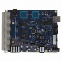
Manufacturer Part Number
C8051F930-TB
Description
BOARD TARGET/PROTO W/C8051F930
Manufacturer
Silicon Laboratories Inc
Type
MCUr
Specifications of C8051F930-TB
Contents
Board
Processor To Be Evaluated
C8051F930
Processor Series
C8051F9xx
Data Bus Width
8 bit
Interface Type
I2C, UART, SPI
Maximum Operating Temperature
+ 85 C
Minimum Operating Temperature
- 40 C
Operating Supply Voltage
0.9 V to 3.6 V
Lead Free Status / RoHS Status
Lead free / RoHS Compliant
For Use With/related Products
C8051F930
Lead Free Status / Rohs Status
Lead free / RoHS Compliant
Other names
336-1472


SFR Definition 5.4. ADC0PWR: ADC0 Burst Mode Power-Up Time
SFR Page = 0xF; SFR Address = 0xBA
Name Reserved
Reset
Type
Bit
6:4
3:0
7
Bit
AD0PWR[3:0]
Reserved
Unused
Name
R
7
0
Reserved.
Read = 0b; Must write 0b.
Unused.
Read = 0000b; Write = Don’t Care.
ADC0 Burst Mode Power-Up Time.
Sets the time delay required for ADC0 to power up from a low power state.
For BURSTEN = 0:
For BURSTEN = 1 and AD0EN = 1:
For BURSTEN = 1 and AD0EN = 0:
R
6
0
ADC0 power state controlled by AD0EN.
ADC0 remains enabled and does not enter a low power state after all conver-
sions are complete.
Conversions can begin immediately following the start-of-conversion signal.
ADC0 enters a low power state (as specified in Table 5.1) after all conversions
are complete.
Conversions can begin a programmed delay after the start-of-conversion sig-
nal.
The ADC0 Burst Mode Power-Up time is programmed according to the follow-
ing equation:
or
AD0PWR
Tstartup
R
5
0
=
=
Tstartup
---------------------- 1
AD0PWR
400ns
Rev. 1.1
R
4
0
–
+
1
C8051F93x-C8051F92x
400ns
Function
3
1
AD0PWR[3:0]
2
1
R/W
1
1
0
1
75
Related parts for C8051F930-TB
Image
Part Number
Description
Manufacturer
Datasheet
Request
R

Part Number:
Description:
SMD/C°/SINGLE-ENDED OUTPUT SILICON OSCILLATOR
Manufacturer:
Silicon Laboratories Inc
Part Number:
Description:
Manufacturer:
Silicon Laboratories Inc
Datasheet:
Part Number:
Description:
N/A N/A/SI4010 AES KEYFOB DEMO WITH LCD RX
Manufacturer:
Silicon Laboratories Inc
Datasheet:
Part Number:
Description:
N/A N/A/SI4010 SIMPLIFIED KEY FOB DEMO WITH LED RX
Manufacturer:
Silicon Laboratories Inc
Datasheet:
Part Number:
Description:
N/A/-40 TO 85 OC/EZLINK MODULE; F930/4432 HIGH BAND (REV E/B1)
Manufacturer:
Silicon Laboratories Inc
Part Number:
Description:
EZLink Module; F930/4432 Low Band (rev e/B1)
Manufacturer:
Silicon Laboratories Inc
Part Number:
Description:
I°/4460 10 DBM RADIO TEST CARD 434 MHZ
Manufacturer:
Silicon Laboratories Inc
Part Number:
Description:
I°/4461 14 DBM RADIO TEST CARD 868 MHZ
Manufacturer:
Silicon Laboratories Inc
Part Number:
Description:
I°/4463 20 DBM RFSWITCH RADIO TEST CARD 460 MHZ
Manufacturer:
Silicon Laboratories Inc
Part Number:
Description:
I°/4463 20 DBM RADIO TEST CARD 868 MHZ
Manufacturer:
Silicon Laboratories Inc
Part Number:
Description:
I°/4463 27 DBM RADIO TEST CARD 868 MHZ
Manufacturer:
Silicon Laboratories Inc
Part Number:
Description:
I°/4463 SKYWORKS 30 DBM RADIO TEST CARD 915 MHZ
Manufacturer:
Silicon Laboratories Inc
Part Number:
Description:
N/A N/A/-40 TO 85 OC/4463 RFMD 30 DBM RADIO TEST CARD 915 MHZ
Manufacturer:
Silicon Laboratories Inc
Part Number:
Description:
I°/4463 20 DBM RADIO TEST CARD 169 MHZ
Manufacturer:
Silicon Laboratories Inc