EVAL-AD7706EB Analog Devices Inc, EVAL-AD7706EB Datasheet - Page 10
EVAL-AD7706EB
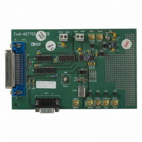
Manufacturer Part Number
EVAL-AD7706EB
Description
BOARD EVAL FOR AD7706
Manufacturer
Analog Devices Inc
Datasheet
1.EVAL-AD7705EB.pdf
(32 pages)
Specifications of EVAL-AD7706EB
Number Of Adc's
1
Number Of Bits
16
Sampling Rate (per Second)
500
Data Interface
Serial
Inputs Per Adc
3 Differential
Input Range
0 ~ 5.25 V
Power (typ) @ Conditions
6.5mW @ 500SPS
Voltage Supply Source
Single
Operating Temperature
-40°C ~ 85°C
Utilized Ic / Part
AD7706
Lead Free Status / RoHS Status
Contains lead / RoHS non-compliant


AD7705/AD7706
ON-CHIP REGISTERS
The AD7705/AD7706 contains eight on-chip registers which can be accessed via the serial port of the part. The first of these is a
Communications Register that controls the channel selection, decides whether the next operation is a read or write operation and
also decides which register the next read or write operation accesses. All communications to the part must start with a write opera-
tion to the Communications Register. After power-on or RESET, the device expects a write to its Communications Register. The
data written to this register determines whether the next operation to the part is a read or a write operation and also determines to
which register this read or write operation occurs. Therefore, write access to any of the other registers on the part starts with a write
operation to the Communications Register followed by a write to the selected register. A read operation from any other register on
the part (including the Communications Register itself and the output data register) starts with a write operation to the Communica-
tions Register followed by a read operation from the selected register. The Communications Register also controls the standby mode
and channel selection and the DRDY status is also available by reading from the Communications Register. The second register is a
Setup Register that determines calibration mode, gain setting, bipolar/unipolar operation and buffered mode. The third register is
labelled the Clock Register and contains the filter selection bits and clock control bits. The fourth register is the Data Register from
which the output data from the part is accessed. The final registers are the calibration registers which store channel calibration data.
The registers are discussed in more detail in the following sections.
Communications Register (RS2, RS1, RS0 = 0, 0, 0)
The Communications Register is an 8-bit register from which data can either be read or to which data can be written. All communi-
cations to the part must start with a write operation to the Communications Register. The data written to the Communications Reg-
ister determines whether the next operation is a read or write operation and to which register this operation takes place. Once the
subsequent read or write operation to the selected register is complete, the interface returns to where it expects a write operation to
the Communications Register. This is the default state of the interface, and on power-up or after a RESET, the AD7705/AD7706 is
in this default state waiting for a write operation to the Communications Register. In situations where the interface sequence is lost,
if a write operation of sufficient duration (containing at least 32 serial clock cycles) takes place with DIN high, the AD7705 returns
to this default state. Table V outlines the bit designations for the Communications Register.
0/DRDY
RS2–RS0
0/DRDY (0)
Figure 8. Typical Crystal Oscillator Power-Up Time
1
2
2
CH1 5.00V
TEK STOP: SINGLE SEQ 50.0kS/s
V
DD
For a write operation, a “0” must be written to this bit so that the write operation to the Communications Register
actually takes place. If a “1” is written to this bit, the part will not clock on to subsequent bits in the register. It
will stay at this bit location until a “0” is written to this bit. Once a “0” is written to this bit, the next seven bits
will be loaded to the Communications Register. For a read operation, this bit provides the status of the DRDY flag
from the part. The status of this bit is the same as the DRDY output pin.
Register Selection Bits. These three bits select to which one of eight on-chip registers the next read or write opera-
tion takes place, as shown in Table VI, along with the register size. When the read or write operation to the se-
lected register is complete, the part returns to where it is waiting for a write operation to the Communications
Register. It does not remain in a state where it will continue to access the register.
OSCILLATOR = 4.9152 MHz
OSCILLATOR = 2.4576 MHz
RS2 (0)
CH2 2.00V
RS1 (0)
Table V. Communications Register
5ms/DIV
RS0 (0)
–10–
R/W (0)
Figure 9. Standby Current vs. Temperature
20
16
12
8
4
0
–40
–30 –20 –10
STBY (0)
MCLK IN = 0V OR V
V
DD
= 3V
0
TEMPERATURE – C
10
20
DD
CH1 (0)
30
V
40
DD
= 5V
50
60
70
CH0 (0)
80
REV. A
Related parts for EVAL-AD7706EB
Image
Part Number
Description
Manufacturer
Datasheet
Request
R

Part Number:
Description:
ENERCHIP CC EVAL KIT
Manufacturer:
Cymbet Corporation
Datasheet:

Part Number:
Description:
BOARD EVAL FOR AD976
Manufacturer:
Analog Devices Inc
Datasheet:

Part Number:
Description:
BOARD EVAL FOR ADXL345
Manufacturer:
Analog Devices Inc
Datasheet:

Part Number:
Description:
ENERCHIP CC SEH EVAL KIT
Manufacturer:
Cymbet Corporation
Datasheet:

Part Number:
Description:
ENERCHIP EP ENERGY HARVEST EVAL
Manufacturer:
Cymbet Corporation
Datasheet:

Part Number:
Description:
EVAL BOARD FOR TW6864-LB2-GR
Manufacturer:
Intersil
Datasheet:
Part Number:
Description:
EVAL BOARD FOR TW8816-LB3-GR
Manufacturer:
Intersil
Datasheet:
Part Number:
Description:
EVAL BOARD FOR TW8817-TA3-GRS
Manufacturer:
Intersil
Datasheet:

Part Number:
Description:
EVALUATION MODULE FOR ADUM4160
Manufacturer:
Analog Devices Inc
Datasheet:

Part Number:
Description:
BOARD EVALUATION ADCMP581BCP
Manufacturer:
Analog Devices Inc
Datasheet:
Part Number:
Description:
BOARD EVALUATION ADM1041
Manufacturer:
Analog Devices Inc
Datasheet:

Part Number:
Description:
EVAL BOARD FOR STM32F107VCT
Manufacturer:
STMicroelectronics
Datasheet:
Part Number:
Description:
BOARD EVAL FOR AD1954
Manufacturer:
Analog Devices Inc
Datasheet:
Part Number:
Description:
BOARD EVAL FOR AD1955
Manufacturer:
Analog Devices Inc
Datasheet:

Part Number:
Description:
BOARD EVAL FOR AD7655
Manufacturer:
Analog Devices Inc
Datasheet: