EVAL-AD7706EB Analog Devices Inc, EVAL-AD7706EB Datasheet - Page 18
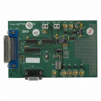
EVAL-AD7706EB
Manufacturer Part Number
EVAL-AD7706EB
Description
BOARD EVAL FOR AD7706
Manufacturer
Analog Devices Inc
Datasheet
1.EVAL-AD7705EB.pdf
(32 pages)
Specifications of EVAL-AD7706EB
Number Of Adc's
1
Number Of Bits
16
Sampling Rate (per Second)
500
Data Interface
Serial
Inputs Per Adc
3 Differential
Input Range
0 ~ 5.25 V
Power (typ) @ Conditions
6.5mW @ 500SPS
Voltage Supply Source
Single
Operating Temperature
-40°C ~ 85°C
Utilized Ic / Part
AD7706
Lead Free Status / RoHS Status
Contains lead / RoHS non-compliant


AD7705/AD7706
The cutoff frequency of the digital filter is determined by the
value loaded to bits FS0 to FS1 in the CLOCK Register. Pro-
gramming a different cutoff frequency via FS0 and FS1 does not
alter the profile of the filter response, it changes the frequency of
the notches. The output update of the part and the frequency of
the first notch correspond.
Since the AD7705/AD7706 contains this on-chip, low-pass
filtering, a settling time is associated with step function inputs
and data on the output will be invalid after a step change until
the settling time has elapsed. The settling time depends upon
the output rate chosen for the filter. The settling time of the
filter to a full-scale step input can be up to four times the output
data period. For a synchronized step input (using the FSYNC
function), the settling time is three times the output data period.
Post-Filtering
The on-chip modulator provides samples at a 19.2 kHz output
rate with f
mates these samples to provide data at an output rate that corre-
sponds to the programmed output rate of the filter. Since the
output data rate is higher than the Nyquist criterion, the output
rate for a given bandwidth will satisfy most application require-
ments. There may, however, be some applications which require
a higher data rate for a given bandwidth and noise performance.
Applications that need this higher data rate will require some
post-filtering following the digital filter of the AD7705/AD7706.
For example, if the required bandwidth is 7.86 Hz, but the
required update rate is 100 Hz, the data can be taken from the
AD7705/AD7706 at the 100 Hz rate giving a –3 dB bandwidth
of 26.2 Hz. Post-filtering can be applied to this to reduce the
bandwidth and output noise, to the 7.86 Hz bandwidth level,
while maintaining an output rate of 100 Hz.
Post-filtering can also be used to reduce the output noise from
the device for bandwidths below 13.1 Hz. At a gain of 128 and
a bandwidth of 13.1 Hz, the output rms noise is 450 nV. This
is essentially device noise or white noise and since the input is
chopped, the noise has a primarily flat frequency response. By
reducing the bandwidth below 13.1 Hz, the noise in the result-
ant passband can be reduced. A reduction in bandwidth by a
factor of 2 results in a reduction of approximately 1.25 in the
output rms noise. This additional filtering will result in a longer
settling-time.
Figure 12. Frequency Response of AD7705 Filter
–100
–120
–140
–160
–180
–200
–220
–240
–20
–40
–60
–80
0
CLKIN
0
at 2.4576 MHz. The on-chip digital filter deci-
60
120
FREQUENCY – Hz
180
240
300
360
–18–
ANALOG FILTERING
The digital filter does not provide any rejection at integer mul-
tiples of the modulator sample frequency, as outlined earlier.
However, due to the AD7705/AD7706’s high oversampling
ratio, these bands occupy only a small fraction of the spectrum
and most broadband noise is filtered. This means that the ana-
log filtering requirements in front of the AD7705/AD7706 are
considerably reduced versus a conventional converter with no
on-chip filtering. In addition, because the part’s common-mode
rejection performance of 100 dB extends out to several kHz,
common-mode noise in this frequency range will be substan-
tially reduced.
Depending on the application, however, it may be necessary to
provide attenuation prior to the AD7705/AD7706 in order to
eliminate unwanted frequencies from these bands which the
digital filter will pass. It may also be necessary in some applica-
tions to provide analog filtering in front of the AD7705/AD7706
to ensure that differential noise signals outside the band of inter-
est do not saturate the analog modulator.
If passive components are placed in front of the AD7705/AD7706
in unbuffered mode, care must be taken to ensure that the
source impedance is low enough not to introduce gain errors in
the system. This significantly limits the amount of passive anti-
aliasing filtering which can be provided in front of the AD7705/
AD7706 when it is used in unbuffered mode. However, when
the part is used in buffered mode, large source impedances will
simply result in a small dc offset error (a 10 k source resistance
will cause an offset error of less than 10 V). Therefore, if the
system requires any significant source impedances to provide
passive analog filtering in front of the AD7705/AD7706, it is
recommended that the part be operated in buffered mode.
CALIBRATION
The AD7705/AD7706 provides a number of calibration options
which can be programmed via the MD1 and MD0 bits of the
Setup Register. The different calibration options are outlined in
the Setup Register and Calibration Sequences sections. A cali-
bration cycle may be initiated at any time by writing to these
bits of the Setup Register. Calibration on the AD7705/AD7706
removes offset and gain errors from the device. A calibration
routine should be initiated on the device whenever there is a
change in the ambient operating temperature or supply voltage.
It should also be initiated if there is a change in the selected
gain, filter notch or bipolar/unipolar input range.
The AD7705/AD7706 offers self-calibration and system calibra-
tion facilities. For full calibration to occur on the selected chan-
nel, the on-chip microcontroller must record the modulator
output for two different input conditions. These are “zero-
scale” and “full-scale” points. These points are derived by
performing a conversion on the different input voltages provided
to the input of the modulator during calibration. As a result, the
accuracy of the calibration can only be as good as the noise level
that it provides in normal mode. The result of the “zero-scale”
calibration conversion is stored in the Zero-Scale Calibration
Register while the result of the “full-scale” calibration conver-
sion is stored in the Full-Scale Calibration Register. With these
readings, the microcontroller can calculate the offset and the
gain slope for the input-to-output transfer function of the con-
verter. Internally, the part works with a resolution of 33 bits to
determine its conversion result of 16 bits.
REV. A
Related parts for EVAL-AD7706EB
Image
Part Number
Description
Manufacturer
Datasheet
Request
R

Part Number:
Description:
ENERCHIP CC EVAL KIT
Manufacturer:
Cymbet Corporation
Datasheet:

Part Number:
Description:
BOARD EVAL FOR AD976
Manufacturer:
Analog Devices Inc
Datasheet:

Part Number:
Description:
BOARD EVAL FOR ADXL345
Manufacturer:
Analog Devices Inc
Datasheet:

Part Number:
Description:
ENERCHIP CC SEH EVAL KIT
Manufacturer:
Cymbet Corporation
Datasheet:

Part Number:
Description:
ENERCHIP EP ENERGY HARVEST EVAL
Manufacturer:
Cymbet Corporation
Datasheet:

Part Number:
Description:
EVAL BOARD FOR TW6864-LB2-GR
Manufacturer:
Intersil
Datasheet:
Part Number:
Description:
EVAL BOARD FOR TW8816-LB3-GR
Manufacturer:
Intersil
Datasheet:
Part Number:
Description:
EVAL BOARD FOR TW8817-TA3-GRS
Manufacturer:
Intersil
Datasheet:

Part Number:
Description:
EVALUATION MODULE FOR ADUM4160
Manufacturer:
Analog Devices Inc
Datasheet:

Part Number:
Description:
BOARD EVALUATION ADCMP581BCP
Manufacturer:
Analog Devices Inc
Datasheet:
Part Number:
Description:
BOARD EVALUATION ADM1041
Manufacturer:
Analog Devices Inc
Datasheet:

Part Number:
Description:
EVAL BOARD FOR STM32F107VCT
Manufacturer:
STMicroelectronics
Datasheet:
Part Number:
Description:
BOARD EVAL FOR AD1954
Manufacturer:
Analog Devices Inc
Datasheet:
Part Number:
Description:
BOARD EVAL FOR AD1955
Manufacturer:
Analog Devices Inc
Datasheet:

Part Number:
Description:
BOARD EVAL FOR AD7655
Manufacturer:
Analog Devices Inc
Datasheet: