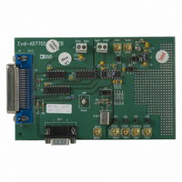
EVAL-AD7706EB Analog Devices Inc, EVAL-AD7706EB Datasheet - Page 12
EVAL-AD7706EB
Manufacturer Part Number
EVAL-AD7706EB
Description
BOARD EVAL FOR AD7706
Manufacturer
Analog Devices Inc
Datasheet
1.EVAL-AD7705EB.pdf
(32 pages)
Specifications of EVAL-AD7706EB
Number Of Adc's
1
Number Of Bits
16
Sampling Rate (per Second)
500
Data Interface
Serial
Inputs Per Adc
3 Differential
Input Range
0 ~ 5.25 V
Power (typ) @ Conditions
6.5mW @ 500SPS
Voltage Supply Source
Single
Operating Temperature
-40°C ~ 85°C
Utilized Ic / Part
AD7706
Lead Free Status / RoHS Status
Contains lead / RoHS non-compliant


AD7705/AD7706
Setup Register (RS2, RS1, RS0 = 0, 0, 1); Power-On/Reset Status: 01 Hex
The Setup Register is an eight bit register from which data can either be read or to which data can be written. Table IX outlines the
bit designations for the Setup Register.
MD1
0
0
1
1
G2–G0
B/U
BUF
FSYNC
MD1 (0)
MD0
0
1
0
1
Gain Selection Bits. These bits select the gain setting for the on-chip PGA as outlined in Table X.
Bipolar/Unipolar Operation. A “0” in this bit selects Bipolar Operation. A “1” in this bit selects Unipolar Operation.
Buffer Control. With this bit at “0,” the on-chip buffer on the analog input is shorted out. With the buffer shorted
out, the current flowing in the V
analog input allowing the input to handle higher source impedances.
Filter Synchronization. When this bit is high, the nodes of the digital filter, the filter control logic and the calibra-
tion control logic are held in a reset state and the analog modulator is also held in its reset state. When this bit
goes low, the modulator and filter start to process data and a valid word is available in 3 1/(output update rate),
i.e., the settling time of the filter. This FSYNC bit does not affect the digital interface and does not reset the
DRDY output if it is low.
MD0 (0)
Operating Mode
Normal Mode: this is the normal mode of operation of the device whereby the device is performing normal
conversions.
Self-Calibration: this activates self-calibration on the channel selected by CH1 and CH0 of the Communica-
tions Register. This is a one-step calibration sequence and when complete the part returns to Normal Mode
with MD1 and MD0 returning to 0, 0. The DRDY output or bit goes high when calibration is initiated and
returns low when this self-calibration is complete and a new valid word is available in the data register. The
zero-scale calibration is performed at the selected gain on internally shorted (zeroed) inputs and the full-
scale calibration is performed at the selected gain on an internally-generated V
Zero-Scale System Calibration: this activates zero scale system calibration on the channel selected by CH1
and CH0 of the Communications Register. Calibration is performed at the selected gain on the input volt-
age provided at the analog input during this calibration sequence. This input voltage should remain stable
for the duration of the calibration. The DRDY output or bit goes high when calibration is initiated and
returns low when this zero-scale calibration is complete and a new valid word is available in the data register.
At the end of the calibration, the part returns to Normal Mode with MD1 and MD0 returning to 0, 0.
Full-Scale System Calibration: this activates full-scale system calibration on the selected input channel.
Calibration is performed at the selected gain on the input voltage provided at the analog input during this
calibration sequence. This input voltage should remain stable for the duration of the calibration. Once
again, the DRDY output or bit goes high when calibration is initiated and returns low when this full-scale
calibration is complete and a new valid word is available in the data register. At the end of the calibration,
the part returns to Normal Mode with MD1 and MD0 returning to 0, 0.
G2
0
0
0
0
1
1
1
1
G2 (0)
G1
0
0
1
1
0
0
1
1
DD
Table IX. Setup Register
line is reduced. When this bit is high, the on-chip buffer is in series with the
Table X. Gain Selection
G1 (0)
–12–
G0
0
1
0
1
0
1
0
1
G0 (0)
Gain Setting
1
2
4
8
16
32
64
128
B/U (0)
REF
BUF (0)
/Selected Gain.
FSYNC (1)
REV. A
Related parts for EVAL-AD7706EB
Image
Part Number
Description
Manufacturer
Datasheet
Request
R

Part Number:
Description:
ENERCHIP CC EVAL KIT
Manufacturer:
Cymbet Corporation
Datasheet:

Part Number:
Description:
BOARD EVAL FOR AD976
Manufacturer:
Analog Devices Inc
Datasheet:

Part Number:
Description:
BOARD EVAL FOR ADXL345
Manufacturer:
Analog Devices Inc
Datasheet:

Part Number:
Description:
ENERCHIP CC SEH EVAL KIT
Manufacturer:
Cymbet Corporation
Datasheet:

Part Number:
Description:
ENERCHIP EP ENERGY HARVEST EVAL
Manufacturer:
Cymbet Corporation
Datasheet:

Part Number:
Description:
EVAL BOARD FOR TW6864-LB2-GR
Manufacturer:
Intersil
Datasheet:
Part Number:
Description:
EVAL BOARD FOR TW8816-LB3-GR
Manufacturer:
Intersil
Datasheet:
Part Number:
Description:
EVAL BOARD FOR TW8817-TA3-GRS
Manufacturer:
Intersil
Datasheet:

Part Number:
Description:
EVALUATION MODULE FOR ADUM4160
Manufacturer:
Analog Devices Inc
Datasheet:

Part Number:
Description:
BOARD EVALUATION ADCMP581BCP
Manufacturer:
Analog Devices Inc
Datasheet:
Part Number:
Description:
BOARD EVALUATION ADM1041
Manufacturer:
Analog Devices Inc
Datasheet:

Part Number:
Description:
EVAL BOARD FOR STM32F107VCT
Manufacturer:
STMicroelectronics
Datasheet:
Part Number:
Description:
BOARD EVAL FOR AD1954
Manufacturer:
Analog Devices Inc
Datasheet:
Part Number:
Description:
BOARD EVAL FOR AD1955
Manufacturer:
Analog Devices Inc
Datasheet:

Part Number:
Description:
BOARD EVAL FOR AD7655
Manufacturer:
Analog Devices Inc
Datasheet: