EVAL-AD7706EB Analog Devices Inc, EVAL-AD7706EB Datasheet - Page 14
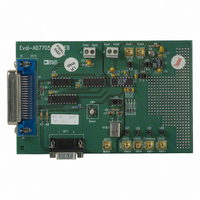
EVAL-AD7706EB
Manufacturer Part Number
EVAL-AD7706EB
Description
BOARD EVAL FOR AD7706
Manufacturer
Analog Devices Inc
Datasheet
1.EVAL-AD7705EB.pdf
(32 pages)
Specifications of EVAL-AD7706EB
Number Of Adc's
1
Number Of Bits
16
Sampling Rate (per Second)
500
Data Interface
Serial
Inputs Per Adc
3 Differential
Input Range
0 ~ 5.25 V
Power (typ) @ Conditions
6.5mW @ 500SPS
Voltage Supply Source
Single
Operating Temperature
-40°C ~ 85°C
Utilized Ic / Part
AD7706
Lead Free Status / RoHS Status
Contains lead / RoHS non-compliant


AD7705/AD7706
Data Register (RS2, RS1, RS0 = 0, 1, 1)
The Data Register on the part is a 16-bit read-only register that contains the most up-to-date conversion result from the AD7705/
AD7706. If the Communications Register sets up the part for a write operation to this register, a write operation must actually take
place to return the part to where it is expecting a write operation to the Communications Register. However, the 16 bits of data
written to the part will be ignored by the AD7705/AD7706.
Test Register (RS2, RS1, RS0 = 1, 0, 0); Power-On/Reset Status: 00 Hex
The part contains a Test Register that is used when testing the device. The user is advised not to change the status of any of the bits
in this register from the default (Power-on or RESET) status of all 0s as the part will be placed in one of its test modes and will not
operate correctly.
Zero-Scale Calibration Register (RS2, RS1, RS0 = 1, 1, 0); Power-On/Reset Status: 1F4000 Hex
The AD7705/AD7706 contains independent sets of zero-scale registers, one for each of the input channels. Each of these registers is
a 24-bit read/write register; 24 bits of data must be written otherwise no data will be transferred to the register. This register is used
in conjunction with its associated full-scale register to form a register pair. These register pairs are associated with input channel
pairs as outlined in Table VII. While the part is set up to allow access to these registers over the digital interface, the part itself no
longer has access to the register coefficients to correctly scale the output data. As a result, there is a possibility that after accessing the
calibration registers (either read or write operation) the first output data read from the part may contain incorrect data. In addition, a
write to the calibration register should not be attempted while a calibration is in progress. These eventualities can be avoided by
taking the FSYNC bit in the mode register high before the calibration register operation and taking it low after the operation is
complete.
Full-Scale Calibration Register (RS2, RS1, RS0 = 1, 1, 1); Power-On/Reset Status: 5761AB Hex
The AD7705/AD7706 contains independent sets of full-scale registers, one for each of the input channels. Each of these registers is a
24-bit read/write register; 24 bits of data must be written otherwise no data will be transferred to the register. This register is used in
conjunction with its associated zero-scale register to form a register pair. These register pairs are associated with input channel pairs
as outlined in Table VII. While the part is set up to allow access to these registers over the digital interface, the part itself no longer
has access to the register coefficients to correctly scale the output data. As a result, there is a possibility that after accessing the cali-
bration registers (either read or write operation) the first output data read from the part may contain incorrect data. In addition, a
write to the calibration register should not be attempted while a calibration is in progress. These eventualities can be avoided by
taking FSYNC bit in the mode register high before the calibration register operation and taking it low after the operation is complete.
CALIBRATION SEQUENCES
The AD7705/AD7706 contains a number of calibration options as previously outlined. Table XIII summarizes the calibration types,
the operations involved and the duration of the operations. There are two methods of determining the end of calibration. The first is
to monitor when DRDY returns low at the end of the sequence. DRDY not only indicates when the sequence is complete, but also
that the part has a valid new sample in its data register. This valid new sample is the result of a normal conversion which follows the
calibration sequence. The second method of determining when calibration is complete is to monitor the MD1 and MD0 bits of the
Setup Register. When these bits return to 0 (0 following a calibration command), it indicates that the calibration sequence is com-
plete. This method does not give any indication of there being a valid new result in the data register. However, it gives an earlier
indication than DRDY that calibration is complete. The duration to when the Mode Bits (MD1 and MD0) return to 0 (0 represents
the duration of the calibration carried out). The sequence to when DRDY goes low also includes a normal conversion and a pipeline
delay, t
in the table.
C
Self-Calibration
ZS System Calibration
FS System Calibration
alibration Type
P
, to correctly scale the results of this first conversion. t
MD1, MD0
0, 1
1, 0
1, 1
Calibration Sequence
Internal ZS Cal @ Selected Gain +
Internal FS Cal @ Selected Gain
ZS Cal on AIN @ Selected Gain
FS Cal on AIN @ Selected Gain
Table XIII. Calibration Sequences
P
will never exceed 2000 t
–14–
Duration to Mode Bits
6
3
3
1/Output Rate
1/Output Rate
1/Output Rate
CLKIN
. The time for both methods is given
Duration to DRDY
4
4
9
1/Output Rate + t
1/Output Rate + t
1/Output Rate + t
REV. A
P
P
P
Related parts for EVAL-AD7706EB
Image
Part Number
Description
Manufacturer
Datasheet
Request
R

Part Number:
Description:
ENERCHIP CC EVAL KIT
Manufacturer:
Cymbet Corporation
Datasheet:

Part Number:
Description:
BOARD EVAL FOR AD976
Manufacturer:
Analog Devices Inc
Datasheet:

Part Number:
Description:
BOARD EVAL FOR ADXL345
Manufacturer:
Analog Devices Inc
Datasheet:

Part Number:
Description:
ENERCHIP CC SEH EVAL KIT
Manufacturer:
Cymbet Corporation
Datasheet:

Part Number:
Description:
ENERCHIP EP ENERGY HARVEST EVAL
Manufacturer:
Cymbet Corporation
Datasheet:

Part Number:
Description:
EVAL BOARD FOR TW6864-LB2-GR
Manufacturer:
Intersil
Datasheet:
Part Number:
Description:
EVAL BOARD FOR TW8816-LB3-GR
Manufacturer:
Intersil
Datasheet:
Part Number:
Description:
EVAL BOARD FOR TW8817-TA3-GRS
Manufacturer:
Intersil
Datasheet:

Part Number:
Description:
EVALUATION MODULE FOR ADUM4160
Manufacturer:
Analog Devices Inc
Datasheet:

Part Number:
Description:
BOARD EVALUATION ADCMP581BCP
Manufacturer:
Analog Devices Inc
Datasheet:
Part Number:
Description:
BOARD EVALUATION ADM1041
Manufacturer:
Analog Devices Inc
Datasheet:

Part Number:
Description:
EVAL BOARD FOR STM32F107VCT
Manufacturer:
STMicroelectronics
Datasheet:
Part Number:
Description:
BOARD EVAL FOR AD1954
Manufacturer:
Analog Devices Inc
Datasheet:
Part Number:
Description:
BOARD EVAL FOR AD1955
Manufacturer:
Analog Devices Inc
Datasheet:

Part Number:
Description:
BOARD EVAL FOR AD7655
Manufacturer:
Analog Devices Inc
Datasheet: