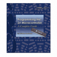
45181 Parallax Inc, 45181 Datasheet - Page 124

45181
Manufacturer Part Number
45181
Description
SX TECH TOOL KIT NO POWER
Manufacturer
Parallax Inc
Series
SXr
Type
Microcontrollerr
Datasheet
1.45180.pdf
(184 pages)
Specifications of 45181
Contents
SX Book, SX Key, SX Tech Board, Samples, Resonators, Cable and Manual
Product
Microcontroller Basic Stamps
Operating Supply Voltage
5 V
For Use With/related Products
SX MCUs
Lead Free Status / RoHS Status
Lead free / RoHS Compliant
- Current page: 124 of 184
- Download datasheet (2Mb)
13 Appendix C: SX Instruction Set
BANK
Operation: Writes file registers bits 7 through 5 (on the SX20/28) or 6 through 4 (on the SX48/52) to the same bits in
CALL
Operation: The next instruction address is pushed onto the stack and addr8 is moved to the program counter. The
CJA
Operation: op1 is compared to op2. If op1 is greater than op2, a jump to addr9 is executed. W is left holding the
Page 124 SX-Key/Blitz Development System Manual 2.0 Parallax, Inc.
BANK
1) CALL
1) CJA
2) CJA
Command
Command
Command
dest
fr
the file select register (FSR) in preparation for a RAM access across a bank boundary. The full 8-bit file
register address must be used as the destination. On the SX48/52, bit 7 in the FSR is used to select between
upper and lower block of banks. This bit is not affected by the BANK instruction, and must be set or cleared with a
separate SETB FSR.7 or CLRB FSR.7 following the BANK instruction.
addr8
addr8
ninth bit of the program counter will be cleared to 0. Therefore, calls are only allowed to the first half of
any 512-word page, although the CALL instruction can be anywhere.
op1, op2, addr9
fr, #literal, addr
fr1, fr2, addr
result of op1 + ~op2 in command #1 and op2 - op1 in command #2. If CARRYX is specified, c affects the
result. Insert a CLC before command #1 and an STC before command #2 to avoid strange results.
Words
Words
Words
1
1
4
4
4 or 6 (jump)
4 or 6 (jump)
(16 or 20)
(16 or 20)
Cycles
Cycles
Cycles
1 (4)
3 (8)
W, C, DC, Z
W, C, DC, Z
Affects
Affects
Affects
FSR
PC
Compare op1 to op2 and jump if above
Call subroutine with 8-bit address
0000 0001 1fff BANK fr
1001 kkkk kkkk CALL addr8
1100 kkkk kkkk MOV W, #lit^$FF
0001 110f ffff ADD W, fr
0110 0000 0011 SNC
101k kkkk kkkk JMP addr9
0010 000f ffff MOV W, fr1
0000 100f ffff MOV W, fr2-W
0111 0000 0011 SC
101k kkkk kkkk JMP addr9
Set bank select bits
Coding
Coding
Coding
Related parts for 45181
Image
Part Number
Description
Manufacturer
Datasheet
Request
R

Part Number:
Description:
Terminals 3 Pin Single Row Header (long)
Manufacturer:
Parallax Inc

Part Number:
Description:
Headers & Wire Housings 16 Pin Single Row Header
Manufacturer:
Parallax Inc

Part Number:
Description:
Microcontroller Modules & Accessories DISCONTINUED BY PARALLAX
Manufacturer:
Parallax Inc

Part Number:
Description:
BOOK UNDERSTANDING SIGNALS
Manufacturer:
Parallax Inc
Datasheet:

Part Number:
Description:
COMPETITION RING FOR SUMOBOT
Manufacturer:
Parallax Inc
Datasheet:

Part Number:
Description:
TEXT INFRARED REMOTE FOR BOE-BOT
Manufacturer:
Parallax Inc
Datasheet:

Part Number:
Description:
Microcontroller Modules & Accessories DISCONTINUED BY PARALLAX
Manufacturer:
Parallax Inc

Part Number:
Description:
BOOK UNDERSTANDING SIGNALS
Manufacturer:
Parallax Inc
Datasheet:

Part Number:
Description:
BOARD EXPERIMENT+LCD NX-1000
Manufacturer:
Parallax Inc
Datasheet:

Part Number:
Description:
IC MCU 2K FLASH 50MHZ SO-18
Manufacturer:
Parallax Inc
Datasheet:


