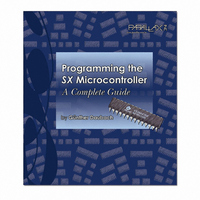
45181 Parallax Inc, 45181 Datasheet - Page 150

45181
Manufacturer Part Number
45181
Description
SX TECH TOOL KIT NO POWER
Manufacturer
Parallax Inc
Series
SXr
Type
Microcontrollerr
Datasheet
1.45180.pdf
(184 pages)
Specifications of 45181
Contents
SX Book, SX Key, SX Tech Board, Samples, Resonators, Cable and Manual
Product
Microcontroller Basic Stamps
Operating Supply Voltage
5 V
For Use With/related Products
SX MCUs
Lead Free Status / RoHS Status
Lead free / RoHS Compliant
- Current page: 150 of 184
- Download datasheet (2Mb)
15 Appendix E: SX Data Sheet
* RA4 – RA7 is only available on the SX52, RD0 – RE7 are only available on the SX48/52,
15.2 Architecture
The Ubicom SX chip offers 2K x 12 internal EE/Flash program memory (4K x 12 in the SX48/52) and up
to 137 bytes of general purpose RAM memory (262 bytes in the SX48/52). The EE/Flash memory is
organized in 512-word pages. The RAM memory is addressable directly or indirectly (as well as semi-
directly in the SX48/52). All special function registers are mapped into the data memory. Configuration
registers do not appear in data memory and are only accessible through the use of the MODE register
and the port configuration commands.
The ALU is 8-bits wide and is capable of arithmetic and Boolean operations. The ‘W’ register is the
working register for the ALU. Typically, it holds one operand in a two-operand instruction. Depending
on the instruction executed, the ALU may affect the values of the Carry (C), Zero (Z), and Digit Carry
(DC) flags of the STATUS register.
The SX chip comes equipped with special features that reduce system cost and power requirements.
The Power-On Reset (POR) and Device Reset Timer eliminate the need for external reset circuitry. The
power saving SLEEP mode, watchdog timer, and code protect features reduce system cost and improve
system integrity.
Page 150 SX-Key/Blitz Development System Manual 2.0 Parallax, Inc.
RA0 – RA7*
RC0 - RC7*
RD0 – RE7*
RB0 - RB2
RB3 - RB7
RC0 – RC7 is not available on the SX18/20
Name
MCLR
RTCC
OSC1
OSC2
Vdd
Vss
Type
I/O
I/O
I/O
I/O
I/O
I/O
P
P
I
I
I
TTL/CMOS/ST
TTL/CMOS/ST
TTL/CMOS/ST
TTL/CMOS/ST
Input Levels
TTL/CMOS
CMOS
ST
ST
ST
-
-
Bi-directional I/O Pin, Complimentary Drive
Bi-directional I/O Pin; MIWU mode; Comparator output,
- input, + input
Bi-directional I/O Pin; MIWU mode; (SX48/52 RB4 – RB7: T1 capture
input 1, 2, PWM/compare out, ext. clock source)
Bi-directional I/O Pin (SX48/52 RC0 – RC3: T2 capture input 1, 2,
PWM/compare out, external clock source)
Bi-directional I/O Pin
Input to Real Time Clock/Counter
Master Clear (reset) input (active low).
Oscillator crystal input - external clock input.
Weakly pulled to Vdd internally on RC mode.
Positive supply for logic and I/O pins.
Ground Reference for logic and I/O pins.
Description
Table 29 - SX Pins
Related parts for 45181
Image
Part Number
Description
Manufacturer
Datasheet
Request
R

Part Number:
Description:
Terminals 3 Pin Single Row Header (long)
Manufacturer:
Parallax Inc

Part Number:
Description:
Headers & Wire Housings 16 Pin Single Row Header
Manufacturer:
Parallax Inc

Part Number:
Description:
Microcontroller Modules & Accessories DISCONTINUED BY PARALLAX
Manufacturer:
Parallax Inc

Part Number:
Description:
BOOK UNDERSTANDING SIGNALS
Manufacturer:
Parallax Inc
Datasheet:

Part Number:
Description:
COMPETITION RING FOR SUMOBOT
Manufacturer:
Parallax Inc
Datasheet:

Part Number:
Description:
TEXT INFRARED REMOTE FOR BOE-BOT
Manufacturer:
Parallax Inc
Datasheet:

Part Number:
Description:
Microcontroller Modules & Accessories DISCONTINUED BY PARALLAX
Manufacturer:
Parallax Inc

Part Number:
Description:
BOOK UNDERSTANDING SIGNALS
Manufacturer:
Parallax Inc
Datasheet:

Part Number:
Description:
BOARD EXPERIMENT+LCD NX-1000
Manufacturer:
Parallax Inc
Datasheet:

Part Number:
Description:
IC MCU 2K FLASH 50MHZ SO-18
Manufacturer:
Parallax Inc
Datasheet:


