MCIMX31LITEKITC Freescale Semiconductor, MCIMX31LITEKITC Datasheet - Page 24
MCIMX31LITEKITC
Manufacturer Part Number
MCIMX31LITEKITC
Description
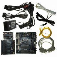
BOARD DEV FOR I.MX31
Manufacturer
Freescale Semiconductor
Type
MCUr
Datasheet
1.MCIMX31LITEKITC.pdf
(122 pages)
Specifications of MCIMX31LITEKITC
Contents
Module and Misc Hardware
For Use With/related Products
i.MX31
Lead Free Status / RoHS Status
Lead free / RoHS Compliant


1
1
Electrical Characteristics
4.3.2
Figure 5
range of operating conditions appears in
Table 19
24
Low-level output current
High-Level DC input voltage
Low-Level DC input voltage
Tri-state leakage current
PA1
Use of DDR Drive can result in excessive overshoot and ringing.
Fast/slow characteristic is selected per GPIO (where available) by “slew rate” control. See reference manual.
ID
Output Transition Times (Max Drive)
Output Transition Times (High Drive)
Output Transition Times (Std Drive)
depicts the load circuit for outputs.
for DDR I/O (unless otherwise noted).
Output (at I/O)
AC Electrical Characteristics
Table 16. DDR (Double Data Rate) I/O DC Electrical Parameters (continued)
Parameter
Table 17. AC Electrical Characteristics of Slow
Parameter
Figure 6. Output Transition Time Waveform
MCIMX31/MCIMX31L Technical Data, Rev. 4.1
CL includes package, probe and fixture capacitance
PA1
Figure 5. Load Circuit for Output
20%
80%
From Output
Table 17
Under Test
Symbol
Figure 6
V
I
V
I
OL
OZ
IH
IL
for slow general I/O,
V
Test Conditions
I
V
depicts the output transition time waveform. The
= NVCC or GND
Symbol
OL
I/O = High Z
DDR Drive
High Drive
Max Drive
Std Drive
Test Point
=0.2*NVCC
tpr
tpr
tpr
CL
—
—
1
Condition
25 pF
50 pF
25 pF
50 pF
25 pF
50 pF
Test
1
PA1
General I/O
0.7*NVCC
Table 18
10.8
14.4
–0.3
Min
3.6
7.2
—
0.92
1.52
2.75
2.79
5.39
Min
1.5
80%
20%
for fast general I/O, and
NVCC NVCC+0.3
1.95
2.98
Typ
Typ
NVCC
0V
—
—
—
—
Freescale Semiconductor
0
0.3*NVCC
16.43
Max
3.17
4.75
4.81
8.42
8.56
Max
±2
—
Units
ns
ns
ns
Units
mA
μA
V
V
Related parts for MCIMX31LITEKITC
Image
Part Number
Description
Manufacturer
Datasheet
Request
R

Part Number:
Description:
Multimedia Applications Processors
Manufacturer:
FREESCALE [Freescale Semiconductor, Inc]
Datasheet:

Part Number:
Description:
Manufacturer:
Freescale Semiconductor, Inc
Datasheet:
Part Number:
Description:
Manufacturer:
Freescale Semiconductor, Inc
Datasheet:
Part Number:
Description:
Manufacturer:
Freescale Semiconductor, Inc
Datasheet:
Part Number:
Description:
Manufacturer:
Freescale Semiconductor, Inc
Datasheet:
Part Number:
Description:
Manufacturer:
Freescale Semiconductor, Inc
Datasheet:
Part Number:
Description:
Manufacturer:
Freescale Semiconductor, Inc
Datasheet:
Part Number:
Description:
Manufacturer:
Freescale Semiconductor, Inc
Datasheet:
Part Number:
Description:
Manufacturer:
Freescale Semiconductor, Inc
Datasheet:
Part Number:
Description:
Manufacturer:
Freescale Semiconductor, Inc
Datasheet:
Part Number:
Description:
Manufacturer:
Freescale Semiconductor, Inc
Datasheet:
Part Number:
Description:
Manufacturer:
Freescale Semiconductor, Inc
Datasheet:
Part Number:
Description:
Manufacturer:
Freescale Semiconductor, Inc
Datasheet:
Part Number:
Description:
Manufacturer:
Freescale Semiconductor, Inc
Datasheet:
Part Number:
Description:
Manufacturer:
Freescale Semiconductor, Inc
Datasheet: