MCIMX31LITEKITC Freescale Semiconductor, MCIMX31LITEKITC Datasheet - Page 90
MCIMX31LITEKITC
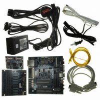
Manufacturer Part Number
MCIMX31LITEKITC
Description
BOARD DEV FOR I.MX31
Manufacturer
Freescale Semiconductor
Type
MCUr
Datasheet
1.MCIMX31LITEKITC.pdf
(122 pages)
Specifications of MCIMX31LITEKITC
Contents
Module and Misc Hardware
For Use With/related Products
i.MX31
Lead Free Status / RoHS Status
Lead free / RoHS Compliant


1
2
3
4
Electrical Characteristics
4.3.20
Each SIM card interface consist of a total of 12 pins (for 2 separate ports of 6 pins each. Mostly one port
with 5 pins is used).
90
Card Input Clock
SDHC Output/Card Inputs CMD, DAT (Reference to CLK)
SDHC Input/Card Outputs CMD, DAT (Reference to CLK)
In low speed mode, card clock must be lower than 400 kHz, voltage ranges from 2.7 V–3.3 V.
In normal data transfer mode for SD/SDIO card, clock frequency can be any value between 0 MHz–25 MHz.
In normal data transfer mode for MMC card, clock frequency can be any value between 0 MHz–20 MHz.
In card identification mode, card clock must be 100 kHz–400 kHz, voltage ranges from 2.7 V–3.3 V.
SD1
SD2
SD3
SD4
SD5
SD6
SD7
SD8
ID
Clock Frequency (Low Speed)
Clock Frequency (SD/SDIO Full Speed)
Clock Frequency (MMC Full Speed)
Clock Frequency (Identification Mode)
Clock Low Time
Clock High Time
Clock Rise Time
Clock Fall Time
SDHC output delay
SDHC input setup
SDHC input hold
SIM Electrical Specifications
DATA[3:0]
DATA[3:0]
CMD
CMD
CLK
Parameter
Table 56. SDHC Interface Timing Parameters
MCIMX31/MCIMX31L Technical Data, Rev. 4.1
Figure 72. SDHC Timing Diagram
SD6
SD7
SD8
SD5
Output from SDHC to card
Input to SDHC
SD1
Symbol
f
t
f
f
f
t
t
t
t
OD
ODL
PP
PP
PP
TLH
THL
WH
t
t
WL
IS
IH
1
2
3
4
SD3
–6.5
Min
100
10
10
—
—
—
—
0
0
0
SD2
Freescale Semiconductor
–11.5
SD4
Max
18.5
400
400
25
20
10
10
—
—
3
Unit
MHz
MHz
kHz
kHz
ns
ns
ns
ns
ns
ns
ns
Related parts for MCIMX31LITEKITC
Image
Part Number
Description
Manufacturer
Datasheet
Request
R

Part Number:
Description:
Multimedia Applications Processors
Manufacturer:
FREESCALE [Freescale Semiconductor, Inc]
Datasheet:

Part Number:
Description:
Manufacturer:
Freescale Semiconductor, Inc
Datasheet:
Part Number:
Description:
Manufacturer:
Freescale Semiconductor, Inc
Datasheet:
Part Number:
Description:
Manufacturer:
Freescale Semiconductor, Inc
Datasheet:
Part Number:
Description:
Manufacturer:
Freescale Semiconductor, Inc
Datasheet:
Part Number:
Description:
Manufacturer:
Freescale Semiconductor, Inc
Datasheet:
Part Number:
Description:
Manufacturer:
Freescale Semiconductor, Inc
Datasheet:
Part Number:
Description:
Manufacturer:
Freescale Semiconductor, Inc
Datasheet:
Part Number:
Description:
Manufacturer:
Freescale Semiconductor, Inc
Datasheet:
Part Number:
Description:
Manufacturer:
Freescale Semiconductor, Inc
Datasheet:
Part Number:
Description:
Manufacturer:
Freescale Semiconductor, Inc
Datasheet:
Part Number:
Description:
Manufacturer:
Freescale Semiconductor, Inc
Datasheet:
Part Number:
Description:
Manufacturer:
Freescale Semiconductor, Inc
Datasheet:
Part Number:
Description:
Manufacturer:
Freescale Semiconductor, Inc
Datasheet:
Part Number:
Description:
Manufacturer:
Freescale Semiconductor, Inc
Datasheet: