MCIMX31LITEKITC Freescale Semiconductor, MCIMX31LITEKITC Datasheet - Page 9
MCIMX31LITEKITC
Manufacturer Part Number
MCIMX31LITEKITC
Description
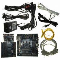
BOARD DEV FOR I.MX31
Manufacturer
Freescale Semiconductor
Type
MCUr
Datasheet
1.MCIMX31LITEKITC.pdf
(122 pages)
Specifications of MCIMX31LITEKITC
Contents
Module and Misc Hardware
For Use With/related Products
i.MX31
Lead Free Status / RoHS Status
Lead free / RoHS Compliant


3
Signal descriptions are in the reference manual. Special signal considerations are listed following this
paragraph. The BGA ball assignment is in
Special Signal Considerations:
Freescale Semiconductor
•
•
•
•
•
•
•
Signal Descriptions
Tamper detect (GPIO1_6)
Tamper detect logic is used to issue a security violation. This logic is activated if the tamper detect
input is asserted.
The tamper detect logic is disabled after reset. After enabling the logic, it is impossible to disable
it until the next reset. The GPR[16] bit functions as the tamper detect enable bit.
GPIO1_6 functions similarly to other I/O with GPIO capabilities regardless of the status of the
tamper detect enable bit. (For example, the GPIO1_6 can function as an input with GPIO
capabilities, such as sampling through PSR or generating interrupts.)
Power ready (GPIO1_5)
The power ready input, GPIO1_5, should be connected to an external power management IC power
ready output signal. If not used, GPIO1_5 must either be (a) externally pulled-up to NVCC1 or (b)
a no connect, internally pulled-up by enabling the on-chip pull-up resistor. GPIO1_5 is a dedicated
input and cannot be used as a general-purpose input/output.
SJC_MOD
SJC_MOD must be externally connected to GND for normal operation. Termination to GND
through an external pull-down resistor (such as 1 kΩ) is allowed, but the value should be much
smaller than the on-chip 100 kΩ pull-up.
CE_CONTROL
CE_CONTROL is a reserved input and must be externally tied to GND through a 1 kΩ resistor.
TTM_PAD
TTM_PAD is for Freescale factory use only. Control bits indicate pull-up/down disabled. However,
TTM_PAD is actually connected to an on-chip pull-down device. Users must either float this signal
or tie it to GND.
M_REQUEST and M_GRANT
These two signals are not utilized internally. The user should make no connection to these signals.
Clock Source Select (CLKSS)
The CLKSS is the input that selects the default reference clock source providing input to the DPLL.
To select CKIH, tie CLKSS to NVCC1. To select CKIL, tie CLKSS to ground. After initialization,
the reference clock source can be changed (initial setting is overwritten) by programming the
PRCS bits in the CCMR.
MCIMX31/MCIMX31L Technical Data, Rev. 4.1
Section 5, “Package Information and
Pinout.”
Signal Descriptions
9
Related parts for MCIMX31LITEKITC
Image
Part Number
Description
Manufacturer
Datasheet
Request
R

Part Number:
Description:
Multimedia Applications Processors
Manufacturer:
FREESCALE [Freescale Semiconductor, Inc]
Datasheet:

Part Number:
Description:
Manufacturer:
Freescale Semiconductor, Inc
Datasheet:
Part Number:
Description:
Manufacturer:
Freescale Semiconductor, Inc
Datasheet:
Part Number:
Description:
Manufacturer:
Freescale Semiconductor, Inc
Datasheet:
Part Number:
Description:
Manufacturer:
Freescale Semiconductor, Inc
Datasheet:
Part Number:
Description:
Manufacturer:
Freescale Semiconductor, Inc
Datasheet:
Part Number:
Description:
Manufacturer:
Freescale Semiconductor, Inc
Datasheet:
Part Number:
Description:
Manufacturer:
Freescale Semiconductor, Inc
Datasheet:
Part Number:
Description:
Manufacturer:
Freescale Semiconductor, Inc
Datasheet:
Part Number:
Description:
Manufacturer:
Freescale Semiconductor, Inc
Datasheet:
Part Number:
Description:
Manufacturer:
Freescale Semiconductor, Inc
Datasheet:
Part Number:
Description:
Manufacturer:
Freescale Semiconductor, Inc
Datasheet:
Part Number:
Description:
Manufacturer:
Freescale Semiconductor, Inc
Datasheet:
Part Number:
Description:
Manufacturer:
Freescale Semiconductor, Inc
Datasheet:
Part Number:
Description:
Manufacturer:
Freescale Semiconductor, Inc
Datasheet: