MCIMX31LITEKITC Freescale Semiconductor, MCIMX31LITEKITC Datasheet - Page 67
MCIMX31LITEKITC
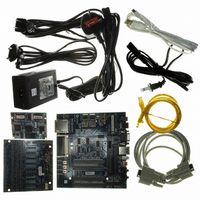
Manufacturer Part Number
MCIMX31LITEKITC
Description
BOARD DEV FOR I.MX31
Manufacturer
Freescale Semiconductor
Type
MCUr
Datasheet
1.MCIMX31LITEKITC.pdf
(122 pages)
Specifications of MCIMX31LITEKITC
Contents
Module and Misc Hardware
For Use With/related Products
i.MX31
Lead Free Status / RoHS Status
Lead free / RoHS Compliant


4.3.15.4.2
The timing characteristics of the TV encoder interface are identical to the synchronous display
characteristics. See
Characteristics.”
4.3.15.5 Asynchronous Interfaces
4.3.15.5.1
The IPU supports the following asynchronous parallel interfaces:
For each of four system interfaces, there are three burst modes:
Both system 80 and system 68k interfaces are supported for all described modes as depicted in
Figure
DISPB_D#_WR and DISPB_D#_RD signals.
Additionally, the IPU allows a programmable pause between two burst. The pause is defined in the
HSP_CLK cycles. It allows to avoid timing violation between two sequential bursts or two accesses to
different displays. The range of this pause is from 4 to 19 HSP_CLK cycles.
Freescale Semiconductor
•
•
1. Burst mode without a separate clock. The burst length is defined by the corresponding parameters
2. Burst mode with the separate clock DISPB_BCLK. In this mode, data is sampled with the
3. Single access mode. In this mode, slave AHB and DMA burst are broken to single accesses. The
53,
System 80 interface
— Type 1 (sampling with the chip select signal) with and without byte enable signals.
— Type 2 (sampling with the read and write signals) with and without byte enable signals.
System 68k interface
— Type 1 (sampling with the chip select signal) with or without byte enable signals.
— Type 2 (sampling with the read and write signals) with or without byte enable signals.
of the IDMAC (when data is transferred from the system memory) of by the HBURST signal (when
the MCU directly accesses the display via the slave AHB bus). For system 80 and system 68k type
1 interfaces, data is sampled by the CS signal and other control signals changes only when transfer
direction is changed during the burst. For type 2 interfaces, data is sampled by the WR/RD signals
(system 80) or by the ENABLE signal (system 68k) and the CS signal stays active during the whole
burst.
DISPB_BCLK clock. The CS signal stays active during whole burst transfer. Other controls are
changed simultaneously with data when the bus state (read, write or wait) is altered. The CS
signals and other controls move to non-active state after burst has been completed.
data is sampled with CS or other controls according the interface type as described above. All
controls (including CS) become non-active for one display interface clock after each access. This
mode corresponds to the ATI single access mode.
Figure
Interface to a TV Encoder,
Parallel Interfaces,
54, and
Section 4.3.15.2.2, “Interface to Active Matrix TFT LCD Panels, Electrical
Figure
MCIMX31/MCIMX31L Technical Data, Rev. 4.1
55. These timing images correspond to active-low DISPB_D#_CS,
Functional Description
Electrical Characteristics
Electrical Characteristics
Figure
52,
67
Related parts for MCIMX31LITEKITC
Image
Part Number
Description
Manufacturer
Datasheet
Request
R

Part Number:
Description:
Multimedia Applications Processors
Manufacturer:
FREESCALE [Freescale Semiconductor, Inc]
Datasheet:

Part Number:
Description:
Manufacturer:
Freescale Semiconductor, Inc
Datasheet:
Part Number:
Description:
Manufacturer:
Freescale Semiconductor, Inc
Datasheet:
Part Number:
Description:
Manufacturer:
Freescale Semiconductor, Inc
Datasheet:
Part Number:
Description:
Manufacturer:
Freescale Semiconductor, Inc
Datasheet:
Part Number:
Description:
Manufacturer:
Freescale Semiconductor, Inc
Datasheet:
Part Number:
Description:
Manufacturer:
Freescale Semiconductor, Inc
Datasheet:
Part Number:
Description:
Manufacturer:
Freescale Semiconductor, Inc
Datasheet:
Part Number:
Description:
Manufacturer:
Freescale Semiconductor, Inc
Datasheet:
Part Number:
Description:
Manufacturer:
Freescale Semiconductor, Inc
Datasheet:
Part Number:
Description:
Manufacturer:
Freescale Semiconductor, Inc
Datasheet:
Part Number:
Description:
Manufacturer:
Freescale Semiconductor, Inc
Datasheet:
Part Number:
Description:
Manufacturer:
Freescale Semiconductor, Inc
Datasheet:
Part Number:
Description:
Manufacturer:
Freescale Semiconductor, Inc
Datasheet:
Part Number:
Description:
Manufacturer:
Freescale Semiconductor, Inc
Datasheet: