CHIPPROG-40 Phyton Inc, CHIPPROG-40 Datasheet - Page 10
CHIPPROG-40
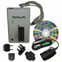
Manufacturer Part Number
CHIPPROG-40
Description
PROGRAMMER STANDALONE 40-DIP
Manufacturer
Phyton Inc
Type
Universal, Stand Aloner
Specifications of CHIPPROG-40
Contents
Programmer, Cables, CD, Power Adapter
Ic Product Type
Programmer, Universal
Ic Interface Type
USB
Features
Embedded Script Language For Automation Of Routine Operations, Splits Files To Multiple Images
Rohs Compliant
Yes
For Use With/related Products
EEPROM, EPROM, FLASH, MCU, NVRAM
Lead Free Status / RoHS Status
Lead free / RoHS Compliant


10
Adapter or Package
adapter
File
Buffer or Memory buffer
Buffer layer or sub-layer
Buffer size
Buffer start address
Checksum
Parallel or In-socket
programming
ICP or in-circuit
programming
ISP or in-circuit
programming
ISP Mode
ChipProg Device Programmers
removing it after completing the programming procedure.-40,
ChipProgChipProg
A small transition board with dual-in-line rows of pins pluggable into the
programmer ZIF socket on the bottom side and with a package-specific ZIF
socket (TSOP, PLCC, etc.) on the top. The adapters for in-system
programming by means of the parallel programmers are implemented as
ribbon cables that connect to the target board via a special header. The
adapter boards can carry passive components (ZIF sockets, pins and
cables) and active components (drivers, latches, transistors, etc.).
Hundreds of Phyton brand adapters as well as third party adapters are
available to support devices in most types of mechanical packages.
In the ChipProg context the term file may represent: a) an image of
information on a PC hard drive or other media that is supposed to be
written into the target device’s physical memory or b) an image read out
from the target device and then stored on the disk or other media. Files in a
ChipProg can be loaded from and saved on a PC hard drive or CD.
A memory segment, physically assigned from the computer operational
memory (RAM), for temporarily storing, editing and displaying the data to
be physically written to the target device’s memory or read out from the
device. The program allows opening an unlimited number of buffers of any
size while it is not restricted by the computer memory.
A buffer may have a few layers (in some topics also known as sub-layers)
that are defined by a particular architecture and memory model of the
target device. For example, for some microcontrollers one buffer can
include the code and data memory layers (see more details below).
The buffers may have different sizes from 128KB to 32GB each.
The address to display the buffer contents from.
An arithmetic sum of the data located within a specified part of the buffer
calculated by the programmer to control the data integrity. The program
enables different algorithms for the checksum calculation and enables
writing the checksum into a specified location of the target device.
Operations on a device being placed into the programmer’s ZIF socket or
into a programming adapter (opposite to the in-system programming
below).
Programming devices mounted on the boards (in the user’s equipment) via
special adapter-cable connecting the programmer to the target.
Same as above. Programming devices mounted on the boards (in the
user’s equipment) via special adapter-cable connecting the programmer
with the target.
Mode of the in-system programming that is usually defined by the
programming signals voltage or the ISP interface (JTAG, UART, SPI, etc.).
Distinct ISP modes are enabled for different target devices and more than
© 2010 Phyton, Inc. Microsystems and Development Tools
Related parts for CHIPPROG-40
Image
Part Number
Description
Manufacturer
Datasheet
Request
R

Part Number:
Description:
Diodes (General Purpose, Power, Switching) HIREL
Manufacturer:
Infineon Technologies
Part Number:
Description:
RF Bipolar Small Signal HIREL
Manufacturer:
Infineon Technologies
Part Number:
Description:
RF Bipolar Small Signal HIREL
Manufacturer:
Infineon Technologies
Part Number:
Description:
RF Bipolar Small Signal HIREL
Manufacturer:
Infineon Technologies