CHIPPROG-40 Phyton Inc, CHIPPROG-40 Datasheet - Page 89
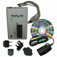
CHIPPROG-40
Manufacturer Part Number
CHIPPROG-40
Description
PROGRAMMER STANDALONE 40-DIP
Manufacturer
Phyton Inc
Type
Universal, Stand Aloner
Specifications of CHIPPROG-40
Contents
Programmer, Cables, CD, Power Adapter
Ic Product Type
Programmer, Universal
Ic Interface Type
USB
Features
Embedded Script Language For Automation Of Routine Operations, Splits Files To Multiple Images
Rohs Compliant
Yes
For Use With/related Products
EEPROM, EPROM, FLASH, MCU, NVRAM
Lead Free Status / RoHS Status
Lead free / RoHS Compliant


© 2010 Phyton, Inc. Microsystems and Development Tools
5.4.1.1
5.4.1.1.1 Managing invalid blocks
5.4.1.1.1.1 Skipping invalid blocks
5.4.1.1.1.2 Reserved Block Area
Read also about
Invalid blocks
NAND Flash memory devices have invalid memory blocks that cannot be used for storing data because
some memory cells inside of the device have physical defects - either inherent in a process of the device
manufacturing or acquired in a process of the device exploitation and reprogramming in the user's
equipment. Since a percentage of invalid blocks is pretty small inside of the chip (usually less than 1%)
it is possible to use the device for data storing. In order to use NAND devices with bad blocks these
blocks should be
document equally uses both known terms for such blocks: invalid and bad.
Locations of the invalid blocks or the invalid blocks map should be accessible by the application for
skipping the bad blocks or handling them in other way. To keep the invalid block map every NAND Flash
device has a special cell array, known as the for storing addresses of invalid blocks. See the Spare
Area location in the
The Spare Area in "small page" 8-bit devices is 16 large, 16-bit devices - 8 Words. The Spare Area in
"large page" devices - 64 Bytes and 32 Words respectfully. Though the Spare Area is dedicated for
marking bad blocks it can be also used as a general purpose memory for storing the user's data. To
avoid accidental losing of the bad block map it is recommended to assign a whole entire Spare Area for
storing the invalid block map and do not write in this area anything else.
This is the simplest method of managing invalid blocks. The programming algorithm first reads the entire
Spare Area
writes data to the device page by page with checking the block addresses. If the current block's number
is marked as bad the programmer skips this block and write into the next valid one.
There are three mostly used methods of handling invalid memory blocks:
Skip Block method
Error Checking and Correction
The ChipProg programmers support all the methods above.
This method is based on the idea of replacing invalid blocks with good blocks by re-directing reading
and writing operations to these good blocks. To implement this method the programming equipment
splits the entire memory in three areas following each other from the start address of the memory
device. Each of these areas may include both good and bad blocks:
User Block Area (UBA) - a linear memory array for storing the user's data;
to collect the addresses of invalid memory blocks. Then, the programming equipment
bad blocks
marked
NAND Flash memory architecture
in a certain way to prevent fetching data from these blocks or writing in it. This
in the NAND Flash memory devices.
Operating with Programmers
89
Related parts for CHIPPROG-40
Image
Part Number
Description
Manufacturer
Datasheet
Request
R

Part Number:
Description:
Diodes (General Purpose, Power, Switching) HIREL
Manufacturer:
Infineon Technologies
Part Number:
Description:
RF Bipolar Small Signal HIREL
Manufacturer:
Infineon Technologies
Part Number:
Description:
RF Bipolar Small Signal HIREL
Manufacturer:
Infineon Technologies
Part Number:
Description:
RF Bipolar Small Signal HIREL
Manufacturer:
Infineon Technologies