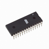
ATMEGA168-20PU Atmel, ATMEGA168-20PU Datasheet - Page 259

ATMEGA168-20PU
Manufacturer Part Number
ATMEGA168-20PU
Description
IC AVR MCU 16K 20MHZ 28DIP
Manufacturer
Atmel
Series
AVR® ATmegar
Datasheets
1.ATAVRTS2080B.pdf
(378 pages)
2.ATMEGA48-20AU.pdf
(35 pages)
3.ATMEGA88-20MU.pdf
(33 pages)
4.ATMEGA168-20AU.pdf
(359 pages)
Specifications of ATMEGA168-20PU
Core Processor
AVR
Core Size
8-Bit
Speed
20MHz
Connectivity
I²C, SPI, UART/USART
Peripherals
Brown-out Detect/Reset, POR, PWM, WDT
Number Of I /o
23
Program Memory Size
16KB (8K x 16)
Program Memory Type
FLASH
Eeprom Size
512 x 8
Ram Size
1K x 8
Voltage - Supply (vcc/vdd)
2.7 V ~ 5.5 V
Data Converters
A/D 6x10b
Oscillator Type
Internal
Operating Temperature
-40°C ~ 85°C
Package / Case
28-DIP (0.300", 7.62mm)
Processor Series
ATMEGA16x
Core
AVR8
Data Bus Width
8 bit
Data Ram Size
1 KB
Interface Type
2-Wire, SPI, USART, Serial
Maximum Clock Frequency
20 MHz
Number Of Programmable I/os
23
Number Of Timers
3
Operating Supply Voltage
2.7 V to 5.5 V
Maximum Operating Temperature
+ 85 C
Mounting Style
Through Hole
3rd Party Development Tools
EWAVR, EWAVR-BL
Development Tools By Supplier
ATAVRDRAGON, ATSTK500, ATSTK600, ATAVRISP2, ATAVRONEKIT
Minimum Operating Temperature
- 40 C
On-chip Adc
10 bit, 6 Channel
A/d Inputs
6-Channel, 10-Bit
Cpu Speed
20 MIPS
Eeprom Memory
512 Bytes
Input Output
23
Interface
I2C/SPI/UART/USART
Memory Type
Flash
Number Of Bits
8
Package Type
28-pin PDIP
Programmable Memory
16K Bytes
Timers
2-8-bit, 1-16-bit
Voltage, Range
4.5-5.5 V
Controller Family/series
AVR MEGA
No. Of I/o's
23
Eeprom Memory Size
512Byte
Ram Memory Size
1KB
Rohs Compliant
Yes
For Use With
ATSTK600-TQFP32 - STK600 SOCKET/ADAPTER 32-TQFPATSTK600 - DEV KIT FOR AVR/AVR32770-1007 - ISP 4PORT ATMEL AVR MCU SPI/JTAGATAVRDRAGON - KIT DRAGON 32KB FLASH MEM AVRATAVRISP2 - PROGRAMMER AVR IN SYSTEMATJTAGICE2 - AVR ON-CHIP D-BUG SYSTEM
Lead Free Status / RoHS Status
Lead free / RoHS Compliant
Available stocks
Company
Part Number
Manufacturer
Quantity
Price
Part Number:
ATMEGA168-20PU
Manufacturer:
ATMEL/爱特梅尔
Quantity:
20 000
- ATAVRTS2080B PDF datasheet
- ATMEGA48-20AU PDF datasheet #2
- ATMEGA88-20MU PDF datasheet #3
- ATMEGA168-20AU PDF datasheet #4
- Current page: 259 of 359
- Download datasheet (3Mb)
23.1.1
2545E–AVR–02/05
Store Program Memory Control and Status Register – SPMCSR
The Store Program Memory Control and Status Register contains the control bits needed to con-
trol the Program memory operations.
• Bit 7 – SPMIE: SPM Interrupt Enable
When the SPMIE bit is written to one, and the I-bit in the Status Register is set (one), the SPM
ready interrupt will be enabled. The SPM ready Interrupt will be executed as long as the SELF-
PRGEN bit in the SPMCSR Register is cleared. The interrupt will not be generated during
EEPROM write or SPM.
• Bit 6 – RWWSB: Read-While-Write Section Busy
This bit is for compatibility with devices supporting Read-While-Write. It will always read as zero
in ATmega48.
• Bit 5 – Res: Reserved Bit
This bit is a reserved bit in the ATmega48/88/168 and will always read as zero.
• Bit 4 – RWWSRE: Read-While-Write Section Read Enable
The functionality of this bit in ATmega48 is a subset of the functionality in ATmega88/168. If the
RWWSRE bit is written while filling the temporary page buffer, the temporary page buffer will be
cleared and the data will be lost.
• Bit 3 – BLBSET: Boot Lock Bit Set
The functionality of this bit in ATmega48 is a subset of the functionality in ATmega88/168. An
LPM instruction within three cycles after BLBSET and SELFPRGEN are set in the SPMCSR
Register, will read either the Lock bits or the Fuse bits (depending on Z0 in the Z-pointer) into the
destination register. See
details.
• Bit 2 – PGWRT: Page Write
If this bit is written to one at the same time as SELFPRGEN, the next SPM instruction within four
clock cycles executes Page Write, with the data stored in the temporary buffer. The page
address is taken from the high part of the Z-pointer. The data in R1 and R0 are ignored. The
PGWRT bit will auto-clear upon completion of a Page Write, or if no SPM instruction is executed
within four clock cycles. The CPU is halted during the entire Page Write operation.
• Bit 1 – PGERS: Page Erase
If this bit is written to one at the same time as SELFPRGEN, the next SPM instruction within four
clock cycles executes Page Erase. The page address is taken from the high part of the Z-
pointer. The data in R1 and R0 are ignored. The PGERS bit will auto-clear upon completion of a
Page Erase, or if no SPM instruction is executed within four clock cycles. The CPU is halted dur-
ing the entire Page Write operation.
Bit
Read/Write
Initial Value
SPMIE
R/W
7
0
RWWSB
R
6
0
”Reading the Fuse and Lock Bits from Software” on page 260
R
5
–
0
RWWSRE
R/W
4
0
BLBSET
R/W
3
0
PGWRT
R/W
2
0
ATmega48/88/168
PGERS
R/W
1
0
SELFPRGEN
R/W
0
0
SPMCSR
259
for
Related parts for ATMEGA168-20PU
Image
Part Number
Description
Manufacturer
Datasheet
Request
R

Part Number:
Description:
Manufacturer:
Atmel Corporation
Datasheet:

Part Number:
Description:
Manufacturer:
Atmel Corporation
Datasheet:

Part Number:
Description:
Manufacturer:
ATMEL Corporation
Datasheet:

Part Number:
Description:
IC AVR MCU 16K 20MHZ 32TQFP
Manufacturer:
Atmel
Datasheet:

Part Number:
Description:
IC AVR MCU 16K 20MHZ 32-QFN
Manufacturer:
Atmel
Datasheet:

Part Number:
Description:
MCU AVR 16K FLASH 15MHZ 32-TQFP
Manufacturer:
Atmel
Datasheet:

Part Number:
Description:
MCU AVR 16K FLASH 15MHZ 32-QFN
Manufacturer:
Atmel
Datasheet:

Part Number:
Description:
IC AVR MCU 16K 20MHZ 32TQFP
Manufacturer:
Atmel
Datasheet:

Part Number:
Description:
MCU AVR 16KB FLASH 20MHZ 32QFN
Manufacturer:
Atmel
Datasheet:

Part Number:
Description:
MCU AVR 16KB FLASH 20MHZ 32TQFP
Manufacturer:
Atmel
Datasheet:

Part Number:
Description:
IC MCU AVR 16K FLASH 32-QFN
Manufacturer:
Atmel
Datasheet:


