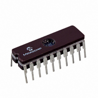
PIC16C771/JW Microchip Technology, PIC16C771/JW Datasheet - Page 111

PIC16C771/JW
Manufacturer Part Number
PIC16C771/JW
Description
IC MCU EPROM4KX14 A/D PWM 20CDIP
Manufacturer
Microchip Technology
Series
PIC® 16Cr
Datasheets
1.PIC16C770-ISO.pdf
(220 pages)
2.PIC16C770-ISO.pdf
(6 pages)
3.PIC16C770-ISO.pdf
(8 pages)
Specifications of PIC16C771/JW
Core Processor
PIC
Core Size
8-Bit
Speed
20MHz
Connectivity
I²C, SPI
Peripherals
Brown-out Detect/Reset, POR, PWM, WDT
Number Of I /o
15
Program Memory Size
7KB (4K x 14)
Program Memory Type
EPROM, UV
Ram Size
256 x 8
Voltage - Supply (vcc/vdd)
4 V ~ 5.5 V
Data Converters
A/D 6x12b
Oscillator Type
External
Operating Temperature
0°C ~ 70°C
Package / Case
20-CDIP (0.300", 7.62mm) Window
For Use With
ISPICR1 - ADAPTER IN-CIRCUIT PROGRAMMINGDVA16XP200 - ADAPTER ICE 20DIP/SOIC/SSOPAC164028 - MODULE SKT PROMATEII 20SOIC/DIP
Lead Free Status / RoHS Status
Contains lead / RoHS non-compliant
Eeprom Size
-
Other names
Q1066306
- Current page: 111 of 220
- Download datasheet (4Mb)
After the A/D module has been configured as desired
and the analog input channels have their correspond-
ing TRIS bits selected for port inputs, the selected
channel must be acquired before conversion is
started. The A/D conversion cycle can be initiated by
setting the GO/DONE bit. The A/D conversion begins
and lasts for 13T
lowed for performing an A/D conversion:
1.
2.
3.
FIGURE 11-3:
2002 Microchip Technology Inc.
Configure port pins:
• Configure Analog Input mode (ANSEL)
• Configure pin as input (TRISA or TRISB)
Configure the A/D module
• Configure A/D Result Format / voltage refer-
• Select A/D input channel (ADCON0)
• Select A/D conversion clock (ADCON0)
• Turn on A/D module (ADCON0)
Configure A/D interrupt (if required)
• Clear ADIF bit
• Set ADIE bit
• Set PEIE bit
• Set GIE bit
C
ence (ADCON1)
ONVERTER
A/D
AD
. The following steps should be fol-
(R
(R
VOLTAGE
A/D BLOCK DIAGRAM
VOLTAGE
EFERENCE
EFERENCE
V
V
REF
REF
-
+
(I
-)
+)
NPUT VOLTAGE
VCFG<2:0>
VCFG<2:0>
V
AIN
)
AV
AV
DD
SS
VRH
VRL
VRL
4.
5.
6.
7.
8.
Clearing the GO/DONE bit during a conversion will
abort the current conversion. The ADRESH and
ADRESL registers will be updated with the partially
completed A/D conversion value. That is, the
ADRESH and ADRESL registers will contain the value
of the current incomplete conversion.
Note:
PIC16C717/770/771
Wait the required acquisition time.
START conversion
• Set GO/DONE bit (ADCON0)
Wait 13T
either:
• Polling for the GO/DONE bit to be cleared
OR
• Waiting for the A/D interrupt
Read A/D Result registers (ADRESH and
ADRESL), clear ADIF if required.
For next conversion, go to step 1, step 2 or step
3 as required.
Do not set the ADON bit and the GO/
DONE bit in the same instruction. Doing so
will cause the GO/DONE bit to be automat-
ically cleared.
CHS<3:0>
AD
until A/D conversion is complete, by
RA1/AN1
RA2/AN2/V
RA0/AN0
RB1/AN5/SS
RB0/AN4/INT
RA3/AN3/V
DS41120B-page 109
REF
REF
-/VRL
+/VRH
Related parts for PIC16C771/JW
Image
Part Number
Description
Manufacturer
Datasheet
Request
R

Part Number:
Description:
IC MCU OTP 8KX14 A/D PWM 44PLCC
Manufacturer:
Microchip Technology
Datasheet:

Part Number:
Description:
IC MCU OTP 8KX14 A/D PWM 44PLCC
Manufacturer:
Microchip Technology
Datasheet:

Part Number:
Description:
IC MCU OTP 8KX14 A/D PWM 44TQFP
Manufacturer:
Microchip Technology
Datasheet:

Part Number:
Description:
IC MCU OTP 8KX14 A/D PWM 44-MQFP
Manufacturer:
Microchip Technology
Datasheet:

Part Number:
Description:
IC MCU OTP 8KX14 A/D PWM 40DIP
Manufacturer:
Microchip Technology
Datasheet:

Part Number:
Description:
IC MCU OTP 8KX14 A/D PWM 44PLCC
Manufacturer:
Microchip Technology
Datasheet:

Part Number:
Description:
IC MCU OTP 8KX14 A/D PWM 40DIP
Manufacturer:
Microchip Technology
Datasheet:

Part Number:
Description:
IC MCU OTP 8KX14 A/D PWM 40DIP
Manufacturer:
Microchip Technology
Datasheet:

Part Number:
Description:
IC MCU OTP 8KX14 A/D PWM 40DIP
Manufacturer:
Microchip Technology
Datasheet:

Part Number:
Description:
IC MCU OTP 8KX14 A/D PWM 44PLCC
Manufacturer:
Microchip Technology
Datasheet:

Part Number:
Description:
IC MCU OTP 8KX14 A/D PWM 44PLCC
Manufacturer:
Microchip Technology
Datasheet:

Part Number:
Description:
IC MCU OTP 8KX14 A/D PWM 44-MQFP
Manufacturer:
Microchip Technology
Datasheet:

Part Number:
Description:
IC MCU OTP 8KX14 A/D PWM 40DIP
Manufacturer:
Microchip Technology
Datasheet:

Part Number:
Description:
IC MCU OTP 8KX14 A/D PWM 44-MQFP
Manufacturer:
Microchip Technology
Datasheet:

Part Number:
Description:
IC MCU OTP 8KX14 A/D PWM 40DIP
Manufacturer:
Microchip Technology
Datasheet:


