PIC16C771/JW Microchip Technology, PIC16C771/JW Datasheet - Page 118
PIC16C771/JW
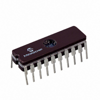
Manufacturer Part Number
PIC16C771/JW
Description
IC MCU EPROM4KX14 A/D PWM 20CDIP
Manufacturer
Microchip Technology
Series
PIC® 16Cr
Datasheets
1.PIC16C770-ISO.pdf
(220 pages)
2.PIC16C770-ISO.pdf
(6 pages)
3.PIC16C770-ISO.pdf
(8 pages)
Specifications of PIC16C771/JW
Core Processor
PIC
Core Size
8-Bit
Speed
20MHz
Connectivity
I²C, SPI
Peripherals
Brown-out Detect/Reset, POR, PWM, WDT
Number Of I /o
15
Program Memory Size
7KB (4K x 14)
Program Memory Type
EPROM, UV
Ram Size
256 x 8
Voltage - Supply (vcc/vdd)
4 V ~ 5.5 V
Data Converters
A/D 6x12b
Oscillator Type
External
Operating Temperature
0°C ~ 70°C
Package / Case
20-CDIP (0.300", 7.62mm) Window
For Use With
ISPICR1 - ADAPTER IN-CIRCUIT PROGRAMMINGDVA16XP200 - ADAPTER ICE 20DIP/SOIC/SSOPAC164028 - MODULE SKT PROMATEII 20SOIC/DIP
Lead Free Status / RoHS Status
Contains lead / RoHS non-compliant
Eeprom Size
-
Other names
Q1066306


PIC16C717/770/771
11.10 A/D Operation During SLEEP
The A/D module can operate during SLEEP mode. This
requires that the A/D clock source be configured for RC
(ADCS<1:0> = 11b). With the RC clock source
selected, when the GO/DONE bit is set the A/D module
waits one instruction cycle before starting the conver-
sion cycle. This allows the SLEEP instruction to be exe-
cuted, which eliminates all digital switching noise
during the sample and conversion. When the conver-
sion cycle is completed the GO/DONE bit is cleared,
and the result loaded into the ADRESH and ADRESL
registers. If the A/D interrupt is enabled, the device will
wake-up from SLEEP. If the A/D interrupt is not
enabled, the A/D module will then be turned off,
although the ADON bit will remain set.
When the A/D clock source is another clock option (not
RC), a SLEEP instruction causes the present conver-
sion to be aborted and the A/D module is turned off,
though the ADON bit will remain set.
TABLE 11-2:
DS41120B-page 116
Address
0Bh,8Bh,
10Bh,18Bh
0Ch
8Ch
1Eh
9Eh
9Bh
1Fh
9Fh
05h
06h
85h
86h
9Dh
17h
Legend: x = unknown, u = unchanged, - = unimplemented read as ’0’. Shaded cells are not used for A/D conversion.
Name
INTCON
PIR1
PIE1
ADRESH
ADRESL
REFCON
ADCON0
ADCON1
PORTA
PORTB
TRISA
TRISB
ANSEL
CCP1CON
SUMMARY OF A/D REGISTERS
A/D High Byte Result Register
A/D Low Byte Result Register
PORTA Data Latch when written: PORTA pins when read
PORTB Data Latch when written: PORTB pins when read
PORTA Data Direction Register
PORTB Data Direction Register
VRHEN
ADCS1
ADFM
Bit 7
GIE
—
—
—
—
VRLEN
ADCS0
VCFG2
Bit 6
PEIE
ADIF
ADIE
—
—
VRHOEN
VCFG1
CHS2
ANS5
Bit 5
T0IE
—
—
—
VRLOEN
VCFG0
CHS1
ANS4
Bit 4
INTE
—
—
—
SSPIF
SSPIE
CHS0
ANS3
Bit 3
RBIE
Turning off the A/D places the A/D module in its lowest
current consumption state.
11.11 Connection Considerations
Since the analog inputs employ ESD protection, they
have diodes to V
analog input must be between V
voltage exceeds this range by greater than 0.3V (either
direction), one of the diodes becomes forward biased
and it may damage the device if the input current spec-
ification is exceeded.
An external RC filter is sometimes added for anti-alias-
ing of the input signal. The R component should be
selected to ensure that the total source impedance is
kept under the 2.5 k recommended specification. It is
recommended that any external components con-
nected to an analog input pin (capacitor, zener diode,
etc.) have very little leakage current.
—
—
Note:
GO/DONE
CCP1IF
CCP1IE
ANS2
Bit 2
T0IF
—
—
For the A/D module to operate in SLEEP,
the A/D clock source must be configured to
RC (ADCS<1:0> = 11).
TMR2IE
TMR2IF
DD
CHS3
ANS1
Bit 1
INTF
—
—
and V
2002 Microchip Technology Inc.
TMR1IE
TMR1IF
ADON
ANS0
Bit 0
RBIF
SS
—
—
. This requires that the
DD
and V
0000 000x
-0-- 0000
-0-- 0000
xxxx xxxx
xxxx xxxx
0000 ----
0000 0000
0000 ----
000x 0000
xxxx xx11
1111 1111
1111 1111
1111 1111
0000 0000
Value on:
POR,
BOR
SS
. If the input
0000 000u
-0-- 0000
-0-- 0000
uuuu uuuu
uuuu uuuu
0000 ----
0000 0000
0000 ----
000u 0000
uuuu uu11
1111 1111
1111 1111
1111 1111
0000 0000
Value on
RESETS
all other
Related parts for PIC16C771/JW
Image
Part Number
Description
Manufacturer
Datasheet
Request
R

Part Number:
Description:
IC MCU OTP 8KX14 A/D PWM 44PLCC
Manufacturer:
Microchip Technology
Datasheet:
Part Number:
Description:
IC MCU OTP 8KX14 A/D PWM 44PLCC
Manufacturer:
Microchip Technology
Datasheet:

Part Number:
Description:
IC MCU OTP 8KX14 A/D PWM 44TQFP
Manufacturer:
Microchip Technology
Datasheet:

Part Number:
Description:
IC MCU OTP 8KX14 A/D PWM 44-MQFP
Manufacturer:
Microchip Technology
Datasheet:

Part Number:
Description:
IC MCU OTP 8KX14 A/D PWM 40DIP
Manufacturer:
Microchip Technology
Datasheet:
Part Number:
Description:
IC MCU OTP 8KX14 A/D PWM 44PLCC
Manufacturer:
Microchip Technology
Datasheet:
Part Number:
Description:
IC MCU OTP 8KX14 A/D PWM 40DIP
Manufacturer:
Microchip Technology
Datasheet:
Part Number:
Description:
IC MCU OTP 8KX14 A/D PWM 40DIP
Manufacturer:
Microchip Technology
Datasheet:
Part Number:
Description:
IC MCU OTP 8KX14 A/D PWM 40DIP
Manufacturer:
Microchip Technology
Datasheet:
Part Number:
Description:
IC MCU OTP 8KX14 A/D PWM 44PLCC
Manufacturer:
Microchip Technology
Datasheet:
Part Number:
Description:
IC MCU OTP 8KX14 A/D PWM 44PLCC
Manufacturer:
Microchip Technology
Datasheet:
Part Number:
Description:
IC MCU OTP 8KX14 A/D PWM 44-MQFP
Manufacturer:
Microchip Technology
Datasheet:
Part Number:
Description:
IC MCU OTP 8KX14 A/D PWM 40DIP
Manufacturer:
Microchip Technology
Datasheet:
Part Number:
Description:
IC MCU OTP 8KX14 A/D PWM 44-MQFP
Manufacturer:
Microchip Technology
Datasheet:
Part Number:
Description:
IC MCU OTP 8KX14 A/D PWM 40DIP
Manufacturer:
Microchip Technology
Datasheet: