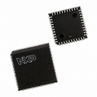
P87C51SBAA,512 NXP Semiconductors, P87C51SBAA,512 Datasheet - Page 24

P87C51SBAA,512
Manufacturer Part Number
P87C51SBAA,512
Description
IC 80C51 MCU 4K OTP 44-PLCC
Manufacturer
NXP Semiconductors
Series
87Cr
Datasheet
1.P87C52UBAA512.pdf
(38 pages)
Specifications of P87C51SBAA,512
Program Memory Type
OTP
Program Memory Size
4KB (4K x 8)
Package / Case
44-PLCC
Core Processor
8051
Core Size
8-Bit
Speed
16MHz
Connectivity
EBI/EMI, UART/USART
Peripherals
POR
Number Of I /o
32
Ram Size
128 x 8
Voltage - Supply (vcc/vdd)
2.7 V ~ 5.5 V
Oscillator Type
Internal
Operating Temperature
0°C ~ 70°C
Processor Series
P87C5x
Core
80C51
Data Bus Width
8 bit
Data Ram Size
128 B
Interface Type
UART
Maximum Clock Frequency
16 MHz
Number Of Programmable I/os
32
Number Of Timers
3
Operating Supply Voltage
2.7 V to 5.5 V
Maximum Operating Temperature
+ 70 C
Mounting Style
SMD/SMT
3rd Party Development Tools
PK51, CA51, A51, ULINK2
Minimum Operating Temperature
0 C
Cpu Family
87C
Device Core
80C51
Device Core Size
8b
Frequency (max)
16MHz
Total Internal Ram Size
128Byte
# I/os (max)
32
Number Of Timers - General Purpose
3
Operating Supply Voltage (typ)
3.3/5V
Operating Supply Voltage (max)
5.5V
Operating Supply Voltage (min)
2.7V
Instruction Set Architecture
CISC
Operating Temp Range
0C to 70C
Operating Temperature Classification
Commercial
Mounting
Surface Mount
Pin Count
44
Package Type
PLCC
Lead Free Status / RoHS Status
Lead free / RoHS Compliant
For Use With
OM10064 - EMULATOR 80C51 PDS51-MK2
Eeprom Size
-
Data Converters
-
Lead Free Status / Rohs Status
Compliant
Other names
568-1246-5
935260182512
P87C51SBAA
935260182512
P87C51SBAA
Available stocks
Company
Part Number
Manufacturer
Quantity
Price
Company:
Part Number:
P87C51SBAA,512
Manufacturer:
NXP Semiconductors
Quantity:
10 000
1. Parameters are valid over operating temperature range unless otherwise specified.
2. Load capacitance for port 0, ALE, and PSEN = 100 pF, load capacitance for all other outputs = 80 pF.
3. Interfacing the 87C51, 80C51, 87C52, or 80C52 to devices with float times up to 45 ns is permitted. This limited bus contention will not
4. See application note AN457 for external memory interface.
5. Parts are guaranteed to operate down to 0 Hz. When an external clock source is used, the RST pin should be held high for a minimum of
Philips Semiconductors
AC ELECTRICAL CHARACTERISTICS
T
NOTES:
2000 Aug 07
amb
1/t
t
t
t
t
t
t
t
t
t
t
t
Data Memory
t
t
t
t
t
t
t
t
t
t
t
t
t
t
External Clock
t
t
t
t
Shift Register
t
t
t
t
t
SYMBOL
LHLL
AVLL
LLAX
LLIV
LLPL
PLPH
PLIV
PXIX
PXIZ
AVIV
PLAZ
RLRH
WLWH
RLDV
RHDX
RHDZ
LLDV
AVDV
LLWL
AVWL
QVWX
WHQX
QVWH
RLAZ
WHLH
CHCX
CLCX
CLCH
CHCL
XLXL
QVXH
XHQX
XHDX
XHDV
80C51 8-bit microcontroller family
4 K/8 K OTP/ROM low voltage (2.7 V–5.5 V),
low power, high speed (33 MHz), 128/256 B RAM
cause damage to Port 0 drivers.
20 s for power-on or wakeup from power down.
CLCL
= 0 C to +70 C or –40 C to +85 C, V
4
FIGURE
15, 16
15, 16
15, 16
15, 16
15, 16
15, 16
15, 16
15, 16
15, 16
15, 16
15, 16
15, 16
15, 16
14
14
14
14
14
14
14
14
14
14
14
14
16
18
18
18
18
17
17
17
17
17
Oscillator frequency
ALE pulse width
Address valid to ALE low
Address hold after ALE low
ALE low to valid instruction in
ALE low to PSEN low
PSEN pulse width
PSEN low to valid instruction in
Input instruction hold after PSEN
Input instruction float after PSEN
Address to valid instruction in
PSEN low to address float
RD pulse width
WR pulse width
RD low to valid data in
Data hold after RD
Data float after RD
ALE low to valid data in
Address to valid data in
ALE low to RD or WR low
Address valid to WR low or RD low
Data valid to WR transition
Data hold after WR
Data valid to WR high
RD low to address float
RD or WR high to ALE high
High time
Low time
Rise time
Fall time
Serial port clock cycle time
Output data setup to clock rising edge
Output data hold after clock rising edge
Input data hold after clock rising edge
Clock rising edge to input data valid
Speed versions :S
CC
PARAMETER
= +2.7 V to +5.5 V, V
5
SS
= 0 V
24
1, 2, 3
16 MHz CLOCK
MIN
142
275
275
137
122
287
750
492
85
22
32
32
13
13
23
20
20
0
0
8
0
MAX
150
207
147
350
397
239
103
492
82
37
10
65
20
20
0
80C51/87C51/80C52/87C52
10t
6t
6t
4t
7t
2t
2t
3t
3t
t
t
t
t
t
t
CLCL
CLCL
CLCL
CLCL
CLCL
CLCL
CLCL
CLCL
CLCL
CLCL
12t
CLCL
CLCL
CLCL
CLCL
CLCL
MIN
3.5
20
20
CLCL
VARIABLE CLOCK
0
0
0
–40
–30
–30
–100
–100
–130
–50
–50
–150
–40
–117
–40
–45
–50
–133
10t
t
t
4t
3t
5t
5t
8t
9t
CLCL
CLCL
2t
3t
t
t
CLCL
CLCL
CLCL
CLCL
CLCL
CLCL
CLCL
CLCL
CLCL
CLCL
CLCL
MAX
16
10
20
20
–t
–t
0
Product specification
–100
–105
–25
–105
–165
–150
–165
+40
CHCX
CLCX
–60
+50
–133
UNIT
MHz
ns
ns
ns
ns
ns
ns
ns
ns
ns
ns
ns
ns
ns
ns
ns
ns
ns
ns
ns
ns
ns
ns
ns
ns
ns
ns
ns
ns
ns
ns
ns
ns
ns
ns


