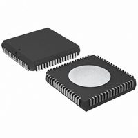
P87C554SBAA,512 NXP Semiconductors, P87C554SBAA,512 Datasheet - Page 19

P87C554SBAA,512
Manufacturer Part Number
P87C554SBAA,512
Description
IC 80C51 MCU 16K OTP 64-PLCC
Manufacturer
NXP Semiconductors
Series
87Cr
Specifications of P87C554SBAA,512
Core Processor
8051
Core Size
8-Bit
Speed
16MHz
Connectivity
EBI/EMI, I²C, UART/USART
Peripherals
POR, PWM, WDT
Number Of I /o
40
Program Memory Size
16KB (16K x 8)
Program Memory Type
OTP
Ram Size
512 x 8
Voltage - Supply (vcc/vdd)
2.7 V ~ 5.5 V
Data Converters
A/D 8x10b
Oscillator Type
Internal
Operating Temperature
0°C ~ 70°C
Package / Case
68-PLCC
Cpu Family
87C
Device Core
80C51
Device Core Size
8b
Frequency (max)
16MHz
Interface Type
I2C/UART
Total Internal Ram Size
512Byte
# I/os (max)
40
Number Of Timers - General Purpose
3
Operating Supply Voltage (typ)
5V
Operating Supply Voltage (max)
5.5V
Operating Supply Voltage (min)
4.5V
On-chip Adc
7-chx10-bit
Instruction Set Architecture
CISC
Operating Temp Range
0C to 70C
Operating Temperature Classification
Commercial
Mounting
Surface Mount
Pin Count
68
Package Type
PLCC
Processor Series
P87C5x
Core
80C51
Data Bus Width
8 bit
Data Ram Size
512 B
Maximum Clock Frequency
16 MHz
Number Of Programmable I/os
40
Number Of Timers
3
Operating Supply Voltage
2.7 V to 5.5 V
Maximum Operating Temperature
+ 70 C
Mounting Style
SMD/SMT
3rd Party Development Tools
PK51, CA51, A51, ULINK2
Minimum Operating Temperature
0 C
Lead Free Status / RoHS Status
Lead free / RoHS Compliant
Eeprom Size
-
Lead Free Status / Rohs Status
Compliant
Other names
568-1254-5
935263385512
P87C554SBAA
935263385512
P87C554SBAA
Available stocks
Company
Part Number
Manufacturer
Quantity
Price
Company:
Part Number:
P87C554SBAA,512
Manufacturer:
NXP Semiconductors
Quantity:
10 000
Philips Semiconductors
Capture Logic: The four 16-bit capture registers that Timer T2 is
connected to are: CT0, CT1, CT2, and CT3. These registers are
loaded with the contents of Timer T2, and an interrupt is requested
upon receipt of the input signals CT0I, CT1I, CT2I, or CT3I. These
input signals are shared with port 1. The four interrupt flags are in
the Timer T2 interrupt register (TM2IR special function register). If
the capture facility is not required, these inputs can be regarded as
additional external interrupt inputs.
Using the capture control register CTCON (see Figure 14), these
inputs may capture on a rising edge, a falling edge, or on either a
rising or falling edge. The inputs are sampled during S1P1 of each
cycle. When a selected edge is detected, the contents of Timer T2
are captured at the end of the cycle.
Measuring Time Intervals Using Capture Registers: When a
recurring external event is represented in the form of rising or falling
edges on one of the four capture pins, the time between two events
2002 Mar 25
80C51 8-bit microcontroller – 12 clock operation
16K/512 OTP/RAM, 8 channel 10-bit A/D, I
capture/compare, high I/O
T2ER
f
RT2
osc
T2
off
STE
TG
TG
S
S
S
S
S
S
External reset
enable
1/12
RTE
R
R
R
R
R
R
T
T
CT0I
CT0
CTI0
INT
P4.0
P4.1
P4.2
P4.3
P4.4
P4.5
P4.6
P4.7
Prescaler
Figure 13. Block Diagram of Timer 2
I/O port 4
CT1I
2
C, PWM,
CT1
CTI1
INT
17
T2 Counter
S
R
T
TG =
can be measured using Timer T2 and a capture register. When an
event occurs, the contents of Timer T2 are copied into the relevant
capture register and an interrupt request is generated. The interrupt
service routine may then compute the interval time if it knows the
previous contents of Timer T2 when the last event occurred. With a
12 MHz oscillator, Timer T2 can be programmed to overflow every
524 ms. When event interval times are shorter than this, computing
the interval time is simple, and the interrupt service routine is short.
For longer interval times, the Timer T2 extension routine may be
used.
Compare Logic: Each time Timer T2 is incremented, the contents
of the three 16-bit compare registers CM0, CM1, and CM2 are
compared with the new counter value of Timer T2. When a match is
found, the corresponding interrupt flag in TM2IR is set at the end of
the following cycle. When a match with CM0 occurs, the controller
sets bits 0-5 of port 4 if the corresponding bits of the set enable
register STE are at logic 1.
=
=
=
set
reset
toggle
toggle status
CMO (S)
COMP
CT2I
8-bit overflow interrupt
16-bit overflow interrupt
CT2
T2 SFR address:
INT
CTI2
INT
CM1 (R)
COMP
TML2
TMH2
INT
=
=
CT3I
lower 8 bits
higher 8 bits
CT3
CM2 (T)
COMP
CTI3
INT
P87C554
Product data
SU00757
INT


