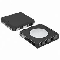
P87C554SBAA,512 NXP Semiconductors, P87C554SBAA,512 Datasheet - Page 73

P87C554SBAA,512
Manufacturer Part Number
P87C554SBAA,512
Description
IC 80C51 MCU 16K OTP 64-PLCC
Manufacturer
NXP Semiconductors
Series
87Cr
Specifications of P87C554SBAA,512
Core Processor
8051
Core Size
8-Bit
Speed
16MHz
Connectivity
EBI/EMI, I²C, UART/USART
Peripherals
POR, PWM, WDT
Number Of I /o
40
Program Memory Size
16KB (16K x 8)
Program Memory Type
OTP
Ram Size
512 x 8
Voltage - Supply (vcc/vdd)
2.7 V ~ 5.5 V
Data Converters
A/D 8x10b
Oscillator Type
Internal
Operating Temperature
0°C ~ 70°C
Package / Case
68-PLCC
Cpu Family
87C
Device Core
80C51
Device Core Size
8b
Frequency (max)
16MHz
Interface Type
I2C/UART
Total Internal Ram Size
512Byte
# I/os (max)
40
Number Of Timers - General Purpose
3
Operating Supply Voltage (typ)
5V
Operating Supply Voltage (max)
5.5V
Operating Supply Voltage (min)
4.5V
On-chip Adc
7-chx10-bit
Instruction Set Architecture
CISC
Operating Temp Range
0C to 70C
Operating Temperature Classification
Commercial
Mounting
Surface Mount
Pin Count
68
Package Type
PLCC
Processor Series
P87C5x
Core
80C51
Data Bus Width
8 bit
Data Ram Size
512 B
Maximum Clock Frequency
16 MHz
Number Of Programmable I/os
40
Number Of Timers
3
Operating Supply Voltage
2.7 V to 5.5 V
Maximum Operating Temperature
+ 70 C
Mounting Style
SMD/SMT
3rd Party Development Tools
PK51, CA51, A51, ULINK2
Minimum Operating Temperature
0 C
Lead Free Status / RoHS Status
Lead free / RoHS Compliant
Eeprom Size
-
Lead Free Status / Rohs Status
Compliant
Other names
568-1254-5
935263385512
P87C554SBAA
935263385512
P87C554SBAA
Available stocks
Company
Part Number
Manufacturer
Quantity
Price
Company:
Part Number:
P87C554SBAA,512
Manufacturer:
NXP Semiconductors
Quantity:
10 000
2. Idle Mode:
3. Power Down Mode:
Philips Semiconductors
2002 Mar 25
80C51 8-bit microcontroller – 12 clock operation
16K/512 OTP/RAM, 8 channel 10-bit A/D, I
capture/compare, high I/O
a. The following pins must be forced to V
b. The following pins must be forced to V
c. Ports 1.6 and 1.7 should be connected to V
d. The following pins must be disconnected: XTAL2 and all pins not specified above.
a. The following pins must be forced to V
b. The following pins must be forced to V
c. Ports 1.6 and 1.7 should be connected to V
d. The following pins must be disconnected: XTAL2 and all pins not specified above.
cannot exceed the I
cannot exceed the I
OL1
OL1
spec of these pins. These pins must not have logic 0 written to them prior to this measurement.
spec of these pins. These pins must not have logic 0 written to them prior to this measurement.
Figure 60. Clock Signal Waveform for I
CLOCK SIGNAL
V
DD
0.5V
–0.5
All other pins are disconnected. V
DD
SS
DD
SS
Figure 61. I
V
: RST, STADC, AV
: RST, STADC, XTAL1, AV
: Port 0 and EW.
: Port 0 and EW.
V
DD
(NC)
DD
(NC)
DD
DD
Figure 59. I
through resistors of sufficiently high value such that the sink current into these pins
through resistors of sufficiently high value such that the sink current into these pins
All other pins are disconnected
0.2V
t
CHCL
0.7V
DD
DD
Test Condition, Power Down Mode
DD
t
2
–0.1
P1.6
P1.7
RST
XTAL2
XTAL1
V
CLCH
P1.6
P1.7
RST
STADC
XTAL2
XTAL1
V
STADC
DD
C, PWM,
SS
SS
Test Condition, Idle Mode
ss
= t
, AV
CHCL
71
t
CLCX
ref–
ss
DD
, and EA.
= 5ns
, AV
t
Tests in Active and Idle Modes
CLCL
AV
AV
AV
AV
ref–
V
V
DD
ref–
ref–
DD
DD
EW
EW
EA
SS
EA
SS
P0
P0
t
, and EA.
CHCX
= 2 V to 5.5 V
t
CLCH
2
I
I
DD
DD
V
V
V
V
SU00220
DD
DD
DD
DD
SU00221
SU00219
3
P87C554
Product data


