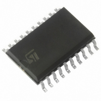
ST7FLIT19BF1M6 STMicroelectronics, ST7FLIT19BF1M6 Datasheet - Page 130

ST7FLIT19BF1M6
Manufacturer Part Number
ST7FLIT19BF1M6
Description
IC MCU 8BIT 4K FLASH 20SOIC
Manufacturer
STMicroelectronics
Series
ST7r
Datasheet
1.ST7FLIT15BY1M6.pdf
(159 pages)
Specifications of ST7FLIT19BF1M6
Core Processor
ST7
Core Size
8-Bit
Speed
8MHz
Connectivity
SPI
Peripherals
LVD, POR, PWM, WDT
Number Of I /o
17
Program Memory Size
4KB (4K x 8)
Program Memory Type
FLASH
Eeprom Size
128 x 8
Ram Size
256 x 8
Voltage - Supply (vcc/vdd)
2.7 V ~ 5.5 V
Data Converters
A/D 7x10b
Oscillator Type
Internal
Operating Temperature
-40°C ~ 85°C
Package / Case
20-SOIC (7.5mm Width)
Processor Series
ST7FLIT1x
Core
ST7
Data Bus Width
8 bit
Data Ram Size
256 B
Interface Type
SPI
Maximum Clock Frequency
8 MHz
Number Of Programmable I/os
17
Number Of Timers
4
Operating Supply Voltage
2.7 V to 5.5 V
Maximum Operating Temperature
+ 85 C
Mounting Style
SMD/SMT
Development Tools By Supplier
ST7FLITE-SK/RAIS, ST7FLIT1B-D/RAIS, ST7MDT10-DVP3, ST7MDT10-EMU3, STX-RLINK
Minimum Operating Temperature
- 40 C
On-chip Adc
10 bit, 7 Channel
For Use With
497-6232 - BOARD EVAL ST7LITE1B,STP5NK60Z497-5049 - KIT STARTER RAISONANCE ST7FLITE497-5046 - KIT TOOL FOR ST7/UPSD/STR7 MCU
Lead Free Status / RoHS Status
Lead free / RoHS Compliant
Other names
497-5627-5
- Current page: 130 of 159
- Download datasheet (3Mb)
ST7LITE1xB
I/O PORT PIN CHARACTERISTICS (Cont’d)
13.8.2 Output Driving Current
Subject to general operating conditions for V
Notes:
1. The I
(I/O ports and control pins) must not exceed I
2. The I
I
3. Not tested in production, based on characterization results.
130/159
IO
Symbol
V
V
V
V
V
V
OH
OH
(I/O ports and control pins) must not exceed I
OL
OL
OH
OL
1)3)
1)3)
2)3)
2)3)
1)
2)
IO
IO
current sourced must always respect the absolute maximum rating specified in
current sunk must always respect the absolute maximum rating specified in
Output low level voltage for a standard I/O pin
when 8 pins are sunk at same time
(see
Output low level voltage for a high sink I/O pin
when 4 pins are sunk at same time
Output high level voltage for an I/O pin
when 4 pins are sourced at same time
Output low level voltage for a standard I/O pin
when 8 pins are sunk at same time
(see
Output low level voltage for a high sink I/O pin
when 4 pins are sunk at same time
Output high level voltage for an I/O pin
when 4 pins are sourced at same time
(see
Output low level voltage for a standard I/O pin
when 8 pins are sunk at same time
(see
Output low level voltage for a high sink I/O pin
when 4 pins are sunk at same time
(see
Output high level voltage for an I/O pin
when 4 pins are sourced at same time
(see
Figure
Figure
Figure
Figure
Figure
Figure
82)
87)
101)
83)
89)
95)
Parameter
VSS
VDD
.
(Figure
DD
.
, f
CPU
94)
, and T
I
I
I
I
I
I
I
I
I
I
I
I
IO
IO
IO
IO
IO
IO
IO
IO
IO
IO
IO
IO
A
=+5mA T
=+2mA T
=+20mA,T
=+8mA T
=-5mA, T
=-2mA T
=+2mA T
=+8mA T
=-2mA T
=+2mA T
=+8mA T
=-2mA T
Conditions
unless otherwise specified.
A
A
A
A
A
A
A
A
A
A
A
A
≤125°C
≤125°C
≤125°C
≤125°C
≤125°C
≤125°C
≤125°C
≤125°C
≤125°C
≤125°C
≤125°C
≤125°C
Section 13.2.2
Section 13.2.2
V
V
V
V
DD
DD
DD
DD
Min
-1.5
-0.8
-0.8
-0.9
and the sum of I
Max
0.75
1.0
0.4
1.3
0.5
0.5
0.6
0.6
and the sum of
Unit
V
IO
Related parts for ST7FLIT19BF1M6
Image
Part Number
Description
Manufacturer
Datasheet
Request
R

Part Number:
Description:
STMicroelectronics [RIPPLE-CARRY BINARY COUNTER/DIVIDERS]
Manufacturer:
STMicroelectronics
Datasheet:

Part Number:
Description:
STMicroelectronics [LIQUID-CRYSTAL DISPLAY DRIVERS]
Manufacturer:
STMicroelectronics
Datasheet:

Part Number:
Description:
BOARD EVAL FOR MEMS SENSORS
Manufacturer:
STMicroelectronics
Datasheet:

Part Number:
Description:
NPN TRANSISTOR POWER MODULE
Manufacturer:
STMicroelectronics
Datasheet:

Part Number:
Description:
TURBOSWITCH ULTRA-FAST HIGH VOLTAGE DIODE
Manufacturer:
STMicroelectronics
Datasheet:

Part Number:
Description:
Manufacturer:
STMicroelectronics
Datasheet:

Part Number:
Description:
DIODE / SCR MODULE
Manufacturer:
STMicroelectronics
Datasheet:

Part Number:
Description:
DIODE / SCR MODULE
Manufacturer:
STMicroelectronics
Datasheet:

Part Number:
Description:
Search -----> STE16N100
Manufacturer:
STMicroelectronics
Datasheet:

Part Number:
Description:
Search ---> STE53NA50
Manufacturer:
STMicroelectronics
Datasheet:

Part Number:
Description:
NPN Transistor Power Module
Manufacturer:
STMicroelectronics
Datasheet:

Part Number:
Description:
DIODE / SCR MODULE
Manufacturer:
STMicroelectronics
Datasheet:


