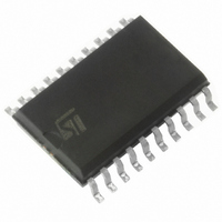
ST7FLIT19BF1M6 STMicroelectronics, ST7FLIT19BF1M6 Datasheet - Page 96

ST7FLIT19BF1M6
Manufacturer Part Number
ST7FLIT19BF1M6
Description
IC MCU 8BIT 4K FLASH 20SOIC
Manufacturer
STMicroelectronics
Series
ST7r
Datasheet
1.ST7FLIT15BY1M6.pdf
(159 pages)
Specifications of ST7FLIT19BF1M6
Core Processor
ST7
Core Size
8-Bit
Speed
8MHz
Connectivity
SPI
Peripherals
LVD, POR, PWM, WDT
Number Of I /o
17
Program Memory Size
4KB (4K x 8)
Program Memory Type
FLASH
Eeprom Size
128 x 8
Ram Size
256 x 8
Voltage - Supply (vcc/vdd)
2.7 V ~ 5.5 V
Data Converters
A/D 7x10b
Oscillator Type
Internal
Operating Temperature
-40°C ~ 85°C
Package / Case
20-SOIC (7.5mm Width)
Processor Series
ST7FLIT1x
Core
ST7
Data Bus Width
8 bit
Data Ram Size
256 B
Interface Type
SPI
Maximum Clock Frequency
8 MHz
Number Of Programmable I/os
17
Number Of Timers
4
Operating Supply Voltage
2.7 V to 5.5 V
Maximum Operating Temperature
+ 85 C
Mounting Style
SMD/SMT
Development Tools By Supplier
ST7FLITE-SK/RAIS, ST7FLIT1B-D/RAIS, ST7MDT10-DVP3, ST7MDT10-EMU3, STX-RLINK
Minimum Operating Temperature
- 40 C
On-chip Adc
10 bit, 7 Channel
For Use With
497-6232 - BOARD EVAL ST7LITE1B,STP5NK60Z497-5049 - KIT STARTER RAISONANCE ST7FLITE497-5046 - KIT TOOL FOR ST7/UPSD/STR7 MCU
Lead Free Status / RoHS Status
Lead free / RoHS Compliant
Other names
497-5627-5
- Current page: 96 of 159
- Download datasheet (3Mb)
ST7LITE1xB
11.5 10-BIT A/D CONVERTER (ADC)
11.5.1 Introduction
The on-chip Analog to Digital Converter (ADC) pe-
ripheral is a 10-bit, successive approximation con-
verter with internal sample and hold circuitry. This
peripheral has up to 7 multiplexed analog input
channels (refer to device pin out description) that
allow the peripheral to convert the analog voltage
levels from up to 7 different sources.
The result of the conversion is stored in a 10-bit
Data Register. The A/D converter is controlled
through a Control/Status Register.
11.5.2 Main Features
■
■
■
Figure 60. ADC Block Diagram
96/159
1
10-bit conversion
Up to 7 channels with multiplexed input
Linear successive approximation
AIN0
AIN6
AIN1
f
CPU
ANALOG
DIV 2
MUX
EOC SPEED ADON
3
ADCDRH
0
1
AMPSEL
x 1 or
x 8
bit
DIV 4
0
R
ADCDRL
ADC
D9
0
CH2
D8
SLOW
■
■
■
The block diagram is shown in
11.5.3 Functional Description
11.5.3.1 Analog Power Supply
V
ence voltage pins. In some devices (refer to device
pin out description) they are internally connected
to the V
Conversion accuracy may therefore be impacted
by voltage drops and noise in the event of heavily
loaded or badly decoupled power supply lines.
bit
1
0
CH1
D7
HOLD CONTROL
DDA
Data register (DR) which contains the results
Conversion complete status flag
On/off bit (to reduce consumption)
0
CH0
and V
D6
DD
0
f
C
ADC
and V
D5
ADC
ADCCSR
SSA
0
D4
are the high and low level refer-
SS
AMP
CAL
ANALOG TO DIGITAL
pins.
D3
SLOW
CONVERTER
D2
AMP
SEL
Figure
D1
60.
D0
Related parts for ST7FLIT19BF1M6
Image
Part Number
Description
Manufacturer
Datasheet
Request
R

Part Number:
Description:
STMicroelectronics [RIPPLE-CARRY BINARY COUNTER/DIVIDERS]
Manufacturer:
STMicroelectronics
Datasheet:

Part Number:
Description:
STMicroelectronics [LIQUID-CRYSTAL DISPLAY DRIVERS]
Manufacturer:
STMicroelectronics
Datasheet:

Part Number:
Description:
BOARD EVAL FOR MEMS SENSORS
Manufacturer:
STMicroelectronics
Datasheet:

Part Number:
Description:
NPN TRANSISTOR POWER MODULE
Manufacturer:
STMicroelectronics
Datasheet:

Part Number:
Description:
TURBOSWITCH ULTRA-FAST HIGH VOLTAGE DIODE
Manufacturer:
STMicroelectronics
Datasheet:

Part Number:
Description:
Manufacturer:
STMicroelectronics
Datasheet:

Part Number:
Description:
DIODE / SCR MODULE
Manufacturer:
STMicroelectronics
Datasheet:

Part Number:
Description:
DIODE / SCR MODULE
Manufacturer:
STMicroelectronics
Datasheet:

Part Number:
Description:
Search -----> STE16N100
Manufacturer:
STMicroelectronics
Datasheet:

Part Number:
Description:
Search ---> STE53NA50
Manufacturer:
STMicroelectronics
Datasheet:

Part Number:
Description:
NPN Transistor Power Module
Manufacturer:
STMicroelectronics
Datasheet:

Part Number:
Description:
DIODE / SCR MODULE
Manufacturer:
STMicroelectronics
Datasheet:


