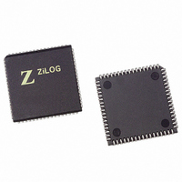
Z8F6422VS020SG Zilog, Z8F6422VS020SG Datasheet - Page 143

Z8F6422VS020SG
Manufacturer Part Number
Z8F6422VS020SG
Description
IC ENCORE MCU FLASH 64K 68PLCC
Manufacturer
Zilog
Series
Encore!® XP®r
Specifications of Z8F6422VS020SG
Core Processor
Z8
Core Size
8-Bit
Speed
20MHz
Connectivity
I²C, IrDA, SPI, UART/USART
Peripherals
Brown-out Detect/Reset, DMA, POR, PWM, WDT
Number Of I /o
46
Program Memory Size
64KB (64K x 8)
Program Memory Type
FLASH
Ram Size
4K x 8
Voltage - Supply (vcc/vdd)
3 V ~ 3.6 V
Data Converters
A/D 12x10b
Oscillator Type
Internal
Operating Temperature
0°C ~ 70°C
Package / Case
68-LCC (J-Lead)
Processor Series
Z8F642x
Core
eZ8
Data Bus Width
8 bit
Data Ram Size
4 KB
Interface Type
I2C, SPI, UART
Maximum Clock Frequency
20 MHz
Number Of Programmable I/os
46
Number Of Timers
4
Operating Supply Voltage
3 V to 3.6 V
Maximum Operating Temperature
+ 70 C
Mounting Style
SMD/SMT
Development Tools By Supplier
Z8F64200100KITG, Z8F64230100ZDF, ZENETSC0100ZACG, ZUSBOPTSC01ZACG, ZUSBSC00100ZACG, Z8F64210100ZDA, Z8F64210100ZDP, Z8F64210100ZDV, Z8F64220100ZDA, Z8F64220100ZDV, Z8F6422AR00ZEM, Z8F6422VS00ZEM, Z8F6421AN00ZEM
Minimum Operating Temperature
0 C
On-chip Adc
10 bit, 12 Channel
For Use With
770-1002 - ISP 4PORT ZILOG Z8 ENCORE! MCU269-4678 - KIT DEV FOR Z8F642 MCU 44 PIN269-4677 - KIT DEV FOR Z8F642 MCU 28PIN269-4643 - KIT DEV Z8 ENCORE XP 28-PIN269-4630 - DEV KIT FOR Z8 ENCORE 8K/4K269-4629 - KIT DEV Z8 ENCORE XP 28-PIN269-4628 - KIT DEV Z8 ENCORE XP 8-PIN269-4540 - KIT DEV FOR Z8 ENCORE 16K TO 64K
Lead Free Status / RoHS Status
Lead free / RoHS Compliant
Eeprom Size
-
Lead Free Status / Rohs Status
Details
Other names
269-4285
Z8F6422VS020SG
Z8F6422VS020SG
Available stocks
Company
Part Number
Manufacturer
Quantity
Price
Company:
Part Number:
Z8F6422VS020SG
Manufacturer:
Zilog
Quantity:
83
Company:
Part Number:
Z8F6422VS020SG
Manufacturer:
Zilog
Quantity:
1 872
- Current page: 143 of 297
- Download datasheet (9Mb)
PS019921-0308
Input Sample Time
(CLKPOL = 0)
(CLKPOL = 1)
Transfer Format PHASE Equals Zero
Figure 24
The two SCK waveforms show polarity with CLKPOL reset to 0 and with CLKPOL set to
one. The diagram may be interpreted as either a Master or Slave timing diagram because
the SCK Master-In/Slave-Out (MISO) and Master-Out/Slave-In (MOSI) pins are directly
connected between the Master and the Slave.
Transfer Format PHASE Equals One
Figure 25
one. Two waveforms are depicted for SCK, one for CLKPOL reset to 0 and another for
CLKPOL set to 1.
MOSI
MISO
SCK
SCK
SS
displays the timing diagram for an SPI transfer in which PHASE is cleared to 0.
on page 130 displays the timing diagram for an SPI transfer in which PHASE is
Bit7
Bit7
Figure 24. SPI Timing When PHASE is 0
Bit6
Bit6
Bit5
Bit5
Bit4
Bit4
Bit3
Bit3
Z8 Encore! XP
Bit2
Bit2
Bit1
Bit1
Product Specification
Serial Peripheral Interface
Bit0
Bit0
®
F64XX Series
129
Related parts for Z8F6422VS020SG
Image
Part Number
Description
Manufacturer
Datasheet
Request
R

Part Number:
Description:
Communication Controllers, ZILOG INTELLIGENT PERIPHERAL CONTROLLER (ZIP)
Manufacturer:
Zilog, Inc.
Datasheet:

Part Number:
Description:
KIT DEV FOR Z8 ENCORE 16K TO 64K
Manufacturer:
Zilog
Datasheet:

Part Number:
Description:
KIT DEV Z8 ENCORE XP 28-PIN
Manufacturer:
Zilog
Datasheet:

Part Number:
Description:
DEV KIT FOR Z8 ENCORE 8K/4K
Manufacturer:
Zilog
Datasheet:

Part Number:
Description:
KIT DEV Z8 ENCORE XP 28-PIN
Manufacturer:
Zilog
Datasheet:

Part Number:
Description:
DEV KIT FOR Z8 ENCORE 4K TO 8K
Manufacturer:
Zilog
Datasheet:

Part Number:
Description:
CMOS Z8 microcontroller. ROM 16 Kbytes, RAM 256 bytes, speed 16 MHz, 32 lines I/O, 3.0V to 5.5V
Manufacturer:
Zilog, Inc.
Datasheet:

Part Number:
Description:
Low-cost microcontroller. 512 bytes ROM, 61 bytes RAM, 8 MHz
Manufacturer:
Zilog, Inc.
Datasheet:

Part Number:
Description:
Z8 4K OTP Microcontroller
Manufacturer:
Zilog, Inc.
Datasheet:

Part Number:
Description:
CMOS SUPER8 ROMLESS MCU
Manufacturer:
Zilog, Inc.
Datasheet:

Part Number:
Description:
SL1866 CMOSZ8 OTP Microcontroller
Manufacturer:
Zilog, Inc.
Datasheet:

Part Number:
Description:
SL1866 CMOSZ8 OTP Microcontroller
Manufacturer:
Zilog, Inc.
Datasheet:

Part Number:
Description:
OTP (KB) = 1, RAM = 125, Speed = 12, I/O = 14, 8-bit Timers = 2, Comm Interfaces Other Features = Por, LV Protect, Voltage = 4.5-5.5V
Manufacturer:
Zilog, Inc.
Datasheet:

Part Number:
Description:
Manufacturer:
Zilog, Inc.
Datasheet:


