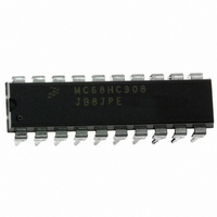
MC68HC908JB8JPE Freescale Semiconductor, MC68HC908JB8JPE Datasheet - Page 147

MC68HC908JB8JPE
Manufacturer Part Number
MC68HC908JB8JPE
Description
IC MCU FLASH 8BIT 8K 20-DIP
Manufacturer
Freescale Semiconductor
Series
HC08r
Datasheet
1.MC908JB8JDWE.pdf
(286 pages)
Specifications of MC68HC908JB8JPE
Core Processor
HC08
Core Size
8-Bit
Speed
3MHz
Connectivity
USB
Peripherals
LVD, POR, PWM
Number Of I /o
13
Program Memory Size
8KB (8K x 8)
Program Memory Type
FLASH
Ram Size
256 x 8
Voltage - Supply (vcc/vdd)
4 V ~ 5.5 V
Oscillator Type
Internal
Operating Temperature
0°C ~ 70°C
Package / Case
20-DIP (0.300", 7.62mm)
Controller Family/series
HC08
No. Of I/o's
13
Ram Memory Size
256Byte
Cpu Speed
3MHz
No. Of Timers
1
Embedded Interface Type
USB
Rohs Compliant
Yes
Processor Series
HC08JB
Core
HC08
Data Bus Width
8 bit
Data Ram Size
256 B
Interface Type
USB
Maximum Clock Frequency
3 MHz
Number Of Programmable I/os
37
Number Of Timers
2
Operating Supply Voltage
4 V to 5.5 V
Maximum Operating Temperature
+ 70 C
Mounting Style
Through Hole
Development Tools By Supplier
FSICEBASE, DEMO908GZ60E, M68EML08GZE, KITUSBSPIDGLEVME, KITUSBSPIEVME, KIT33810EKEVME
Minimum Operating Temperature
0 C
Lead Free Status / RoHS Status
Lead free / RoHS Compliant
Eeprom Size
-
Data Converters
-
Lead Free Status / Rohs Status
Details
- Current page: 147 of 286
- Download datasheet (2Mb)
9.8.7 USB Control Register 2
MC68HC908JB8•MC68HC08JB8•MC68HC08JT8 — Rev. 2.3
Freescale Semiconductor
Address:
FRESUM — Force Resume
TP1SIZ3–TP1SIZ0 — Endpoint 1 Transmit Data Packet Size
T2SEQ — Endpoint 2 Transmit Sequence Bit
Reset:
Read:
Write:
If this bit is 0 or the TXD1F is set, the USB will respond with a NAK
handshake to any endpoint 1 directed IN tokens. Reset clears this bit.
This read/write bit forces a resume state (K or non-idle state) onto the
USB data lines to initiate a remote wakeup. Software should control
the timing of the forced resume to be between 10 and 15 ms. Setting
this bit will not cause the RESUMF bit to be set.
These read/write bits store the number of transmit data bytes for the
next IN token request for endpoint 1. These bits are cleared by reset.
This read/write bit determines which type of data packet (DATA0 or
DATA1) will be sent during the next IN transaction directed to
endpoint 2. Toggling of this bit must be controlled by software. Reset
clears this bit.
1 = Data is ready to be sent
0 = Data is not ready. Respond with NAK
1 = Force data lines to K state
0 = Default
1 = DATA1 token active for next endpoint 2 transmit
0 = DATA0 token active for next endpoint 2 transmit
T2SEQ
$0019
Bit 7
Universal Serial Bus Module (USB)
0
Figure 9-21. USB Control Register 2 (UCR2)
STALL2
6
0
TX2E
5
0
RX2E
4
0
TP2SIZ3
Universal Serial Bus Module (USB)
3
0
TP2SIZ2
2
0
TP2SIZ1
1
0
Technical Data
I/O Registers
TP2SIZ0
Bit 0
0
147
Related parts for MC68HC908JB8JPE
Image
Part Number
Description
Manufacturer
Datasheet
Request
R
Part Number:
Description:
Manufacturer:
Freescale Semiconductor, Inc
Datasheet:
Part Number:
Description:
Manufacturer:
Freescale Semiconductor, Inc
Datasheet:
Part Number:
Description:
Manufacturer:
Freescale Semiconductor, Inc
Datasheet:
Part Number:
Description:
Manufacturer:
Freescale Semiconductor, Inc
Datasheet:
Part Number:
Description:
Manufacturer:
Freescale Semiconductor, Inc
Datasheet:
Part Number:
Description:
Manufacturer:
Freescale Semiconductor, Inc
Datasheet:
Part Number:
Description:
Manufacturer:
Freescale Semiconductor, Inc
Datasheet:
Part Number:
Description:
Manufacturer:
Freescale Semiconductor, Inc
Datasheet:
Part Number:
Description:
Manufacturer:
Freescale Semiconductor, Inc
Datasheet:
Part Number:
Description:
Manufacturer:
Freescale Semiconductor, Inc
Datasheet:
Part Number:
Description:
Manufacturer:
Freescale Semiconductor, Inc
Datasheet:
Part Number:
Description:
Manufacturer:
Freescale Semiconductor, Inc
Datasheet:
Part Number:
Description:
Manufacturer:
Freescale Semiconductor, Inc
Datasheet:
Part Number:
Description:
Manufacturer:
Freescale Semiconductor, Inc
Datasheet:
Part Number:
Description:
Manufacturer:
Freescale Semiconductor, Inc
Datasheet:


