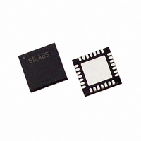
C8051F313-GM Silicon Laboratories Inc, C8051F313-GM Datasheet - Page 209

C8051F313-GM
Manufacturer Part Number
C8051F313-GM
Description
IC 8051 MCU 8K FLASH 28MLP
Manufacturer
Silicon Laboratories Inc
Series
C8051F31xr
Specifications of C8051F313-GM
Core Size
8-Bit
Program Memory Size
8KB (8K x 8)
Oscillator Type
Internal
Core Processor
8051
Speed
25MHz
Connectivity
SMBus (2-Wire/I²C), SPI, UART/USART
Peripherals
POR, PWM, Temp Sensor, WDT
Number Of I /o
25
Program Memory Type
FLASH
Ram Size
1.25K x 8
Voltage - Supply (vcc/vdd)
2.7 V ~ 3.6 V
Data Converters
A/D 17x10b
Operating Temperature
-40°C ~ 85°C
Package / Case
28-VQFN Exposed Pad, 28-HVQFN, 28-SQFN, 28-DHVQFN
No. Of I/o's
25
Ram Memory Size
1280Byte
Cpu Speed
25MHz
No. Of Timers
4
No. Of Pwm Channels
5
Digital Ic Case
RoHS Compliant
Rohs Compliant
Yes
Processor Series
C8051F3x
Core
8051
Data Bus Width
8 bit
Data Ram Size
1.25 KB
Interface Type
I2C, SMBus, SPI, UART
Maximum Clock Frequency
25 MHz
Number Of Programmable I/os
25
Number Of Timers
5
Operating Supply Voltage
2.7 V to 3.6 V
Maximum Operating Temperature
+ 85 C
Mounting Style
SMD/SMT
3rd Party Development Tools
PK51, CA51, A51, ULINK2
Development Tools By Supplier
C8051F310DK
Minimum Operating Temperature
- 40 C
On-chip Adc
10 bit
Data Rom Size
128 B
Height
0.88 mm
Length
5 mm
Supply Voltage (max)
3.6 V
Supply Voltage (min)
2.7 V
Width
5 mm
Lead Free Status / RoHS Status
Lead free / RoHS Compliant
For Use With
770-1006 - ISP 4PORT FOR SILABS C8051F MCU
Eeprom Size
-
Lead Free Status / Rohs Status
Details
Other names
336-1256
- Current page: 209 of 228
- Download datasheet (2Mb)
18.2.4. Frequency Output Mode
Frequency Output Mode produces a programmable-frequency square wave on the module’s associated
CEXn pin. The capture/compare module high byte holds the number of PCA clocks to count before the out-
put is toggled. The frequency of the square wave is then defined by Equation 18.1, where F
quency of the clock selected by the CPS2-0 bits in the PCA mode register, PCA0MD.
Note: A value of 0x00 in the PCA0CPHn register is equal to 256 for this equation.
The lower byte of the capture/compare module is compared to the PCA counter low byte; on a match,
CEXn is toggled and the offset held in the high byte is added to the matched value in PCA0CPLn. Fre-
quency Output Mode is enabled by setting the ECOMn, TOGn, and PWMn bits in the PCA0CPMn register.
PCA0CPLn
Write to
Reset
PCA0CPHn
Write to
0
1
ENB
ENB
Equation 18.1. Square Wave Frequency Output
Figure 18.7. PCA Frequency Output Mode
W
P
M
1
6
n
x
E
C
O
M
n
PCA0CPMn
C
A
P
P
n
0 0 0
C
N
A
P
n
M
A
T
n
O
G
T
n
W
P
M
n
C
C
E
F
n
x
PCA Timebase
F
CEXn
Enable
=
Comparator
PCA0CPLn
---------------------------------------- -
2
Rev. 1.7
PCA0L
8-bit
PCA0CPHn
F
C8051F310/1/2/3/4/5/6/7
PCA
match
Enable
Adder
8-bit Adder
Toggle
TOGn
0
1
CEXn
PCA0CPHn
Crossbar
PCA
is the fre-
Port I/O
209
Related parts for C8051F313-GM
Image
Part Number
Description
Manufacturer
Datasheet
Request
R
Part Number:
Description:
SMD/C°/SINGLE-ENDED OUTPUT SILICON OSCILLATOR
Manufacturer:
Silicon Laboratories Inc
Part Number:
Description:
Manufacturer:
Silicon Laboratories Inc
Datasheet:
Part Number:
Description:
N/A N/A/SI4010 AES KEYFOB DEMO WITH LCD RX
Manufacturer:
Silicon Laboratories Inc
Datasheet:
Part Number:
Description:
N/A N/A/SI4010 SIMPLIFIED KEY FOB DEMO WITH LED RX
Manufacturer:
Silicon Laboratories Inc
Datasheet:
Part Number:
Description:
N/A/-40 TO 85 OC/EZLINK MODULE; F930/4432 HIGH BAND (REV E/B1)
Manufacturer:
Silicon Laboratories Inc
Part Number:
Description:
EZLink Module; F930/4432 Low Band (rev e/B1)
Manufacturer:
Silicon Laboratories Inc
Part Number:
Description:
I°/4460 10 DBM RADIO TEST CARD 434 MHZ
Manufacturer:
Silicon Laboratories Inc
Part Number:
Description:
I°/4461 14 DBM RADIO TEST CARD 868 MHZ
Manufacturer:
Silicon Laboratories Inc
Part Number:
Description:
I°/4463 20 DBM RFSWITCH RADIO TEST CARD 460 MHZ
Manufacturer:
Silicon Laboratories Inc
Part Number:
Description:
I°/4463 20 DBM RADIO TEST CARD 868 MHZ
Manufacturer:
Silicon Laboratories Inc
Part Number:
Description:
I°/4463 27 DBM RADIO TEST CARD 868 MHZ
Manufacturer:
Silicon Laboratories Inc
Part Number:
Description:
I°/4463 SKYWORKS 30 DBM RADIO TEST CARD 915 MHZ
Manufacturer:
Silicon Laboratories Inc
Part Number:
Description:
N/A N/A/-40 TO 85 OC/4463 RFMD 30 DBM RADIO TEST CARD 915 MHZ
Manufacturer:
Silicon Laboratories Inc
Part Number:
Description:
I°/4463 20 DBM RADIO TEST CARD 169 MHZ
Manufacturer:
Silicon Laboratories Inc


