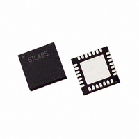
C8051F313-GM Silicon Laboratories Inc, C8051F313-GM Datasheet - Page 34

C8051F313-GM
Manufacturer Part Number
C8051F313-GM
Description
IC 8051 MCU 8K FLASH 28MLP
Manufacturer
Silicon Laboratories Inc
Series
C8051F31xr
Specifications of C8051F313-GM
Core Size
8-Bit
Program Memory Size
8KB (8K x 8)
Oscillator Type
Internal
Core Processor
8051
Speed
25MHz
Connectivity
SMBus (2-Wire/I²C), SPI, UART/USART
Peripherals
POR, PWM, Temp Sensor, WDT
Number Of I /o
25
Program Memory Type
FLASH
Ram Size
1.25K x 8
Voltage - Supply (vcc/vdd)
2.7 V ~ 3.6 V
Data Converters
A/D 17x10b
Operating Temperature
-40°C ~ 85°C
Package / Case
28-VQFN Exposed Pad, 28-HVQFN, 28-SQFN, 28-DHVQFN
No. Of I/o's
25
Ram Memory Size
1280Byte
Cpu Speed
25MHz
No. Of Timers
4
No. Of Pwm Channels
5
Digital Ic Case
RoHS Compliant
Rohs Compliant
Yes
Processor Series
C8051F3x
Core
8051
Data Bus Width
8 bit
Data Ram Size
1.25 KB
Interface Type
I2C, SMBus, SPI, UART
Maximum Clock Frequency
25 MHz
Number Of Programmable I/os
25
Number Of Timers
5
Operating Supply Voltage
2.7 V to 3.6 V
Maximum Operating Temperature
+ 85 C
Mounting Style
SMD/SMT
3rd Party Development Tools
PK51, CA51, A51, ULINK2
Development Tools By Supplier
C8051F310DK
Minimum Operating Temperature
- 40 C
On-chip Adc
10 bit
Data Rom Size
128 B
Height
0.88 mm
Length
5 mm
Supply Voltage (max)
3.6 V
Supply Voltage (min)
2.7 V
Width
5 mm
Lead Free Status / RoHS Status
Lead free / RoHS Compliant
For Use With
770-1006 - ISP 4PORT FOR SILABS C8051F MCU
Eeprom Size
-
Lead Free Status / Rohs Status
Details
Other names
336-1256
- Current page: 34 of 228
- Download datasheet (2Mb)
C8051F310/1/2/3/4/5/6/7
1.8.
C8051F31x devices include two on-chip voltage comparators that are enabled/disabled and configured via
user software. Port I/O pins may be configured as comparator inputs via a selection mux. Two comparator
outputs may be routed to a Port pin if desired: a latched output and/or an unlatched (asynchronous) output.
Comparator response time is programmable, allowing the user to select between high-speed and low-
power modes. Positive and negative hysteresis are also configurable.
Comparator interrupts may be generated on rising, falling, or both edges. When in IDLE mode, these inter-
rupts may be used as a “wake-up” source. Comparator0 may also be configured as a reset source.
Figure 1.16 shows he Comparator0 block diagram.
34
CMX0N1
CMX0N0
CMX0P1
CMX0P0
Comparators
P1.0
P1.4
P2.0
P2.4
P1.1
P1.5
P2.1
P2.5
Figure 1.16. Comparator0 Block Diagram
CP0HYP1
CP0HYP0
CP0HYN1
CP0HYN0
CP0OUT
CP0RIF
CP0EN
CP0FIF
CP0 +
CP0 -
CP0MD1
CP0MD0
CP0RIE
CP0FIE
Rev. 1.7
+
-
GND
VDD
Decision
Reset
Tree
(SYNCHRONIZER)
D
SET
CLR
Q
Q
D
SET
CLR
Q
Q
Rising-edge
CP0
Crossbar
Interrupt
Logic
Falling-edge
Interrupt
CP0
CP0A
CP0
CP0
Related parts for C8051F313-GM
Image
Part Number
Description
Manufacturer
Datasheet
Request
R
Part Number:
Description:
SMD/C°/SINGLE-ENDED OUTPUT SILICON OSCILLATOR
Manufacturer:
Silicon Laboratories Inc
Part Number:
Description:
Manufacturer:
Silicon Laboratories Inc
Datasheet:
Part Number:
Description:
N/A N/A/SI4010 AES KEYFOB DEMO WITH LCD RX
Manufacturer:
Silicon Laboratories Inc
Datasheet:
Part Number:
Description:
N/A N/A/SI4010 SIMPLIFIED KEY FOB DEMO WITH LED RX
Manufacturer:
Silicon Laboratories Inc
Datasheet:
Part Number:
Description:
N/A/-40 TO 85 OC/EZLINK MODULE; F930/4432 HIGH BAND (REV E/B1)
Manufacturer:
Silicon Laboratories Inc
Part Number:
Description:
EZLink Module; F930/4432 Low Band (rev e/B1)
Manufacturer:
Silicon Laboratories Inc
Part Number:
Description:
I°/4460 10 DBM RADIO TEST CARD 434 MHZ
Manufacturer:
Silicon Laboratories Inc
Part Number:
Description:
I°/4461 14 DBM RADIO TEST CARD 868 MHZ
Manufacturer:
Silicon Laboratories Inc
Part Number:
Description:
I°/4463 20 DBM RFSWITCH RADIO TEST CARD 460 MHZ
Manufacturer:
Silicon Laboratories Inc
Part Number:
Description:
I°/4463 20 DBM RADIO TEST CARD 868 MHZ
Manufacturer:
Silicon Laboratories Inc
Part Number:
Description:
I°/4463 27 DBM RADIO TEST CARD 868 MHZ
Manufacturer:
Silicon Laboratories Inc
Part Number:
Description:
I°/4463 SKYWORKS 30 DBM RADIO TEST CARD 915 MHZ
Manufacturer:
Silicon Laboratories Inc
Part Number:
Description:
N/A N/A/-40 TO 85 OC/4463 RFMD 30 DBM RADIO TEST CARD 915 MHZ
Manufacturer:
Silicon Laboratories Inc
Part Number:
Description:
I°/4463 20 DBM RADIO TEST CARD 169 MHZ
Manufacturer:
Silicon Laboratories Inc


