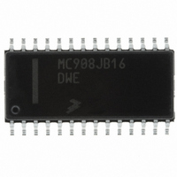
MC908JB16DWE Freescale Semiconductor, MC908JB16DWE Datasheet - Page 252

MC908JB16DWE
Manufacturer Part Number
MC908JB16DWE
Description
IC MCU 16K FLASH 6MHZ USB 28SOIC
Manufacturer
Freescale Semiconductor
Series
HC08r
Specifications of MC908JB16DWE
Core Processor
HC08
Core Size
8-Bit
Speed
6MHz
Connectivity
SCI, USB
Peripherals
LED, LVD, POR, PWM
Number Of I /o
21
Program Memory Size
16KB (16K x 8)
Program Memory Type
FLASH
Ram Size
384 x 8
Voltage - Supply (vcc/vdd)
4 V ~ 5.5 V
Oscillator Type
Internal
Operating Temperature
0°C ~ 70°C
Package / Case
28-SOIC (7.5mm Width)
Processor Series
HC08JB
Core
HC08
Data Bus Width
8 bit
Data Ram Size
384 B
Interface Type
I2C/SCI/SPI/USB
Maximum Clock Frequency
12 MHz
Number Of Programmable I/os
21
Number Of Timers
4
Operating Supply Voltage
5.5 V
Maximum Operating Temperature
+ 70 C
Mounting Style
SMD/SMT
Development Tools By Supplier
FSICEBASE, DEMO908GZ60E, M68EML08GZE, KITUSBSPIDGLEVME, KITUSBSPIEVME, KIT33810EKEVME
Minimum Operating Temperature
0 C
Controller Family/series
HC08
No. Of I/o's
21
Ram Memory Size
384Byte
Cpu Speed
8MHz
No. Of Timers
2
Embedded Interface Type
I2C, SCI, SPI
Rohs Compliant
Yes
Lead Free Status / RoHS Status
Lead free / RoHS Compliant
Eeprom Size
-
Data Converters
-
Lead Free Status / Rohs Status
Lead free / RoHS Compliant
Available stocks
Company
Part Number
Manufacturer
Quantity
Price
Company:
Part Number:
MC908JB16DWE
Manufacturer:
FREESCALE
Quantity:
1 831
Part Number:
MC908JB16DWE
Manufacturer:
FRE/MOT
Quantity:
20 000
- Current page: 252 of 332
- Download datasheet (4Mb)
Clock Generator Module (CGM)
13.4 I/O Signals
13.4.1 CGM Power Supply Pins (V
13.4.2 CGM1 Voltage Regulator Out (V
13.4.3 CGM2 Voltage Regulator In (V
Technical Data
252
The following paragraphs describe the CGM I/O signals.
V
the analog portions of both CGMs.
3.3V output of the on-chip voltage regulator for analog portions. Connect
V
3.3V input for CGM2 analog portions. Connect V
V
DDA
REGA0
REGA1
V
SSA0
is the power supply pin, V
directly to V
as shown in
Clock Generator Module (CGM)
Figure 13-3. CGM Power Supply Connection
C
DDA
C
REGBYPASS
REGBULK
CGM1
> 4.7 µF
0.1 µF
, V
REGA1
+
REGA0
SSA0
REGA1
Figure
)
V
, V
V
REGA0
)
REGA0
SSA1
as shown in
13-3.
)
SSA0
and V
Figure
V
V
REGA1
REGA1
SSA1
MC68HC908JB16
13-3.
are the ground pins for
REGA0
Freescale Semiconductor
C
0.1 µF
> 4.7 µF
+
C
REGBYPASS
REGBULK
CGM2
directly to
—
V
SSA1
Rev. 1.1
Related parts for MC908JB16DWE
Image
Part Number
Description
Manufacturer
Datasheet
Request
R
Part Number:
Description:
Manufacturer:
Freescale Semiconductor, Inc
Datasheet:
Part Number:
Description:
Manufacturer:
Freescale Semiconductor, Inc
Datasheet:
Part Number:
Description:
Manufacturer:
Freescale Semiconductor, Inc
Datasheet:
Part Number:
Description:
Manufacturer:
Freescale Semiconductor, Inc
Datasheet:
Part Number:
Description:
Manufacturer:
Freescale Semiconductor, Inc
Datasheet:
Part Number:
Description:
Manufacturer:
Freescale Semiconductor, Inc
Datasheet:
Part Number:
Description:
Manufacturer:
Freescale Semiconductor, Inc
Datasheet:
Part Number:
Description:
Manufacturer:
Freescale Semiconductor, Inc
Datasheet:
Part Number:
Description:
Manufacturer:
Freescale Semiconductor, Inc
Datasheet:
Part Number:
Description:
Manufacturer:
Freescale Semiconductor, Inc
Datasheet:
Part Number:
Description:
Manufacturer:
Freescale Semiconductor, Inc
Datasheet:
Part Number:
Description:
Manufacturer:
Freescale Semiconductor, Inc
Datasheet:
Part Number:
Description:
Manufacturer:
Freescale Semiconductor, Inc
Datasheet:
Part Number:
Description:
Manufacturer:
Freescale Semiconductor, Inc
Datasheet:
Part Number:
Description:
Manufacturer:
Freescale Semiconductor, Inc
Datasheet:


