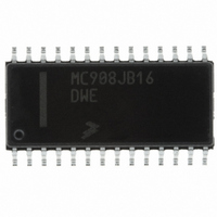
MC908JB16DWE Freescale Semiconductor, MC908JB16DWE Datasheet - Page 304

MC908JB16DWE
Manufacturer Part Number
MC908JB16DWE
Description
IC MCU 16K FLASH 6MHZ USB 28SOIC
Manufacturer
Freescale Semiconductor
Series
HC08r
Specifications of MC908JB16DWE
Core Processor
HC08
Core Size
8-Bit
Speed
6MHz
Connectivity
SCI, USB
Peripherals
LED, LVD, POR, PWM
Number Of I /o
21
Program Memory Size
16KB (16K x 8)
Program Memory Type
FLASH
Ram Size
384 x 8
Voltage - Supply (vcc/vdd)
4 V ~ 5.5 V
Oscillator Type
Internal
Operating Temperature
0°C ~ 70°C
Package / Case
28-SOIC (7.5mm Width)
Processor Series
HC08JB
Core
HC08
Data Bus Width
8 bit
Data Ram Size
384 B
Interface Type
I2C/SCI/SPI/USB
Maximum Clock Frequency
12 MHz
Number Of Programmable I/os
21
Number Of Timers
4
Operating Supply Voltage
5.5 V
Maximum Operating Temperature
+ 70 C
Mounting Style
SMD/SMT
Development Tools By Supplier
FSICEBASE, DEMO908GZ60E, M68EML08GZE, KITUSBSPIDGLEVME, KITUSBSPIEVME, KIT33810EKEVME
Minimum Operating Temperature
0 C
Controller Family/series
HC08
No. Of I/o's
21
Ram Memory Size
384Byte
Cpu Speed
8MHz
No. Of Timers
2
Embedded Interface Type
I2C, SCI, SPI
Rohs Compliant
Yes
Lead Free Status / RoHS Status
Lead free / RoHS Compliant
Eeprom Size
-
Data Converters
-
Lead Free Status / Rohs Status
Lead free / RoHS Compliant
Available stocks
Company
Part Number
Manufacturer
Quantity
Price
Company:
Part Number:
MC908JB16DWE
Manufacturer:
FREESCALE
Quantity:
1 831
Part Number:
MC908JB16DWE
Manufacturer:
FRE/MOT
Quantity:
20 000
- Current page: 304 of 332
- Download datasheet (4Mb)
Low-Voltage Inhibit (LVI)
18.4 Functional Description
18.4.1 Low V
Technical Data
304
DD
Detector
Figure 18-1
out of reset. The LVI module contains independent bandgap reference
circuit and comparator for monitoring the V
voltage. An LVI reset performs a MCU internal reset and drives the RST
pin low to provide low-voltage protection to external peripheral devices.
The low V
reset when the V
in the configuration register (CONFIG) selects the trip point voltage. The
V
See
interaction between the SIM and the LVI.
DD
DETECTOR
DETECTOR
LOW V
LOW V
LVI5OR3
8.4.2.5 Low-Voltage Inhibit (LVI) Reset
LVI circuit can be disabled by the setting the LVID bit in CONFIG.
V
V
DD
REG
REG
DD
DD
shows the structure of the LVI module. The LVI is enabled
detector circuit monitors the V
Low-Voltage Inhibit (LVI)
V
V
V
V
Figure 18-1. LVI Module Block Diagram
DD
DD
DD
DD
DD
> V
< V
> V
< V
LVR
LVR
LVRR
LVRR
voltage falls below the trip voltage. The LVI5OR3 bit
= 0
= 1
= 0
= 1
LVIDR
LVID
DD
DD
voltage and the V
for details of the
voltage and forces a LVI
MC68HC908JB16
Freescale Semiconductor
LVI RESET
—
REG
Rev. 1.1
Related parts for MC908JB16DWE
Image
Part Number
Description
Manufacturer
Datasheet
Request
R
Part Number:
Description:
Manufacturer:
Freescale Semiconductor, Inc
Datasheet:
Part Number:
Description:
Manufacturer:
Freescale Semiconductor, Inc
Datasheet:
Part Number:
Description:
Manufacturer:
Freescale Semiconductor, Inc
Datasheet:
Part Number:
Description:
Manufacturer:
Freescale Semiconductor, Inc
Datasheet:
Part Number:
Description:
Manufacturer:
Freescale Semiconductor, Inc
Datasheet:
Part Number:
Description:
Manufacturer:
Freescale Semiconductor, Inc
Datasheet:
Part Number:
Description:
Manufacturer:
Freescale Semiconductor, Inc
Datasheet:
Part Number:
Description:
Manufacturer:
Freescale Semiconductor, Inc
Datasheet:
Part Number:
Description:
Manufacturer:
Freescale Semiconductor, Inc
Datasheet:
Part Number:
Description:
Manufacturer:
Freescale Semiconductor, Inc
Datasheet:
Part Number:
Description:
Manufacturer:
Freescale Semiconductor, Inc
Datasheet:
Part Number:
Description:
Manufacturer:
Freescale Semiconductor, Inc
Datasheet:
Part Number:
Description:
Manufacturer:
Freescale Semiconductor, Inc
Datasheet:
Part Number:
Description:
Manufacturer:
Freescale Semiconductor, Inc
Datasheet:
Part Number:
Description:
Manufacturer:
Freescale Semiconductor, Inc
Datasheet:


